Showing posts with label DC/DC converter. Show all posts

Monday, June 23, 2014

Safeguarding your power-sensitive DUTs from an over power condition

Today’s system DC power supplies incorporate quite a variety of features to protect both the device under test (DUT) as well as the power supply itself from damage due to a fault condition or setting mishap. Over voltage protect (OVP) and over current protect (OCP) are two core protection features that are found on most all system DC power supplies to help protect against power-related damage.

OVP helps assure the DUT is protected against power-related damage in the event voltage rises above an acceptable range of operation. As over voltage damage is almost instantaneous the OVP level is set at reasonable margin below this level to be effective, yet is suitably higher than maximum expected DUT operating voltage so that any transient voltages do not cause false tripping. Causes of OV conditions are often external to the DUT.

OCP helps assure the DUT is protected against power-related damage in the event it fails in some fashion causing excess current, such as an internal short or some other type of failure. The DUT can also draw excess current from consuming excess power due to overloading or internal problem causing inefficient operation and excessive internal power dissipation.

OVP and OCP are depicted in Figure 1 below for an example DUT that operates at a set voltage level of 48V, within a few percent, and uses about 450W of power. In this case the OVP and OCP levels are set at about 10% higher to safeguard the DUT.


Figure 1: OVP and OCP settings to safeguard an example DUT

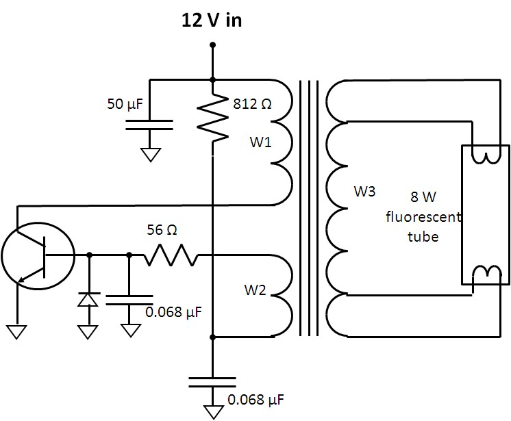
However, not all DUTs operate over as limited a range as depicted in Figure 1. Consider for example many, if not most all DC to DC converters operate over a wide range of voltage while using relatively constant power. Similarly many devices incorporate DC to DC converters to give them an extended range of input voltage operation. To illustrate with an example, consider a DC to DC converter that operates from 24 to 48 volts and runs at 225W is shown in Figure 2. DC to DC converters operate very efficiency so they dissipate a small amount of power and the rest is transferred to the load. If there is a problem with the DC to DC converter causing it to run inefficiently it could be quickly damaged due to overheating. While the fixed OCP level depicted here will also adequately protect it for over power at 24 volts, as can be seen it does not work well to protect the DUT for over power at higher voltage levels.


Figure 2: Example DC to DC converter input V and I operating range

A preferable alternative would instead be to have an over power protection limit, as depicted in Figure 3. This would provide an adequate safeguard regardless of input voltage setting.


Figure 3: Example DC to DC converter input V and I operating range with over power protect

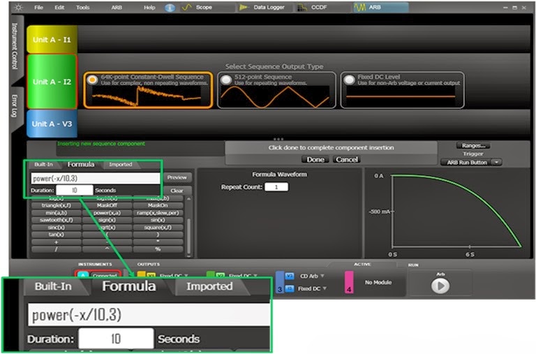
As an over power level setting is not a feature that is commonly found in system DC power supplies, this would then mean having to change the OCP level for each voltage setting change, which may not be convenient or desirable, or in some cases practical to do. However, in the Agilent N6900A and N7900A Advance Power System DC power supplies it is possible to continually sense the output power level in the configurable smart triggering system. This can in turn be used to create a logical expression to use the output power level to trigger an output protect shutdown. This is depicted in Figure 4, using the N7906A software utility to graphically configure this logical expression and then download it into the Advance Power System DC power supply. As the smart triggering system operates at hardware speeds within the instrument it is fast-responding, an important consideration for implementing protection mechanisms.


Figure 4: N7906A Software utility graphically configuring an over power protect shutdown

A glitch delay was also added to prevent false triggers due to temporary peaks of power being drawn by the DUT during transient events. While the output power level is being used here to trigger a fault shutdown it could have been just as easily used to trigger a variety of other actions as well.

Wednesday, May 14, 2014

European Space Power Conference (ESPC) for 2014

This week’s blog posting is going in a bit of a different direction, as I likewise did last month, to attend and participate in the 2014 European Space Power Conference (ESPC) for 2014. While this was the tenth ESPC, which I understand takes place every couple of years; this was the first time I had opportunity to attend. One thing for certain; this was all about DC power, which is directly aligned with the things I am always involved in. In this particular instance it was all about DC power for satellites and space-bound crafts and probes.

I initially found it just a bit curious that a number of the keynote speeches also focused a fair amount on terrestrial solar power as well, but I supposed I should not be at all surprised. There has been a large amount of innovation and a variety of things that benefit our daily lives that came out of our own space program, fueled by our involvement in the “space race” and still continuing on to this day. (Can you name a few by chance?). This is a natural progression for a vast number of technological advances we enjoy.

At ESPC there were numerous papers presented on solar cells and arrays, batteries and energy storage, nuclear power sources, power conversion and DC/DC converters, super-capacitors, and a variety of other topics related to power. Just a couple of my learnings and observations include:
·         There was a very high level of collaboration of sharing findings and answering questions among peers attending the event
·         While batteries generally have very limited lives, from findings presented, it was interesting to see how well they have performed over extended periods in space, lasting last well in excess of their planned life expectancies. It is a reflection of a combination of several things including careful control and workmanship, understanding life-shortening and failure mechanisms, how to take properly treat them over time, what should be expected, as well as other factors contributing to their longevity. I expect this kind of work will ultimately find its way to being applied to using lithium ion batteries in automotive as well.
·         A lot of innovation likewise continues with solar cell development with higher conversion efficiencies coming from multi-junction devices. Maybe we’ll see this become commonplace for terrestrial applications before long!
·         A number of research papers were presented from participants from universities as well. In all, the quality of work was excellent.

I was there with another colleague, Carlo Canziani. Together we represented some of our DC power solutions there, including our N7905A DC Power Analyzer, N7900 series Advanced Power System (APS), and E4360A series Solar Array Simulator (SAS) mainframe and modules. These are the kinds of advanced power stimulus and measurement test instruments vital for conducting testing on satellite and spacecraft power components and systems.

In all it was a refreshing change of pace to be at an event where power is the primary focus, and if this happens to be an area of interest to you as well, you can find out more about ESPC from their site by clicking on the following link: (ESPC2014). Maybe you will find it worthwhile to attend or even present results of some of your work at the next one as well!

Monday, February 24, 2014

How to test the efficiency of DC to DC converters, part 2 of 2

In part 1 of my posting on testing the efficiency of DC to DC converters (click here to review) I went over the test set up, the requirements for load sweep synchronized to the measurements, and details of the choice of the type and set up of the current load sweep itself. In this second part I will be describing details of the measurement set up, setting up the efficiency calculation, and results of the testing. This is based on using the N6705B DC Power Analyzer, N6782A SMUs, and 14585A software as a platform but a number of ideas can be applicable regardless of the platform.


Figure 1: Synchronized measurement and efficiency calculation set up

The synchronized measurement and efficiency calculation set up, and display of results are shown in Figure 1, taking note of the following details corresponding to the numbers in Figure 1:
  1. In the 14585A the data logging mode was selected to make and display the measurements. The oscilloscope mode could have just as easily been used but with a 10 second sweep the extra speed of sampling with the oscilloscope mode was not an advantage. A second thing about using the data logging mode is you can set the integration time period for each acquisition point. This can be used to advantage in averaging out noise and disturbances as needed for a smoother and more representative result. In this case an integration period of 50 milliseconds was used.
  2. To synchronize the measurements the data log measurement was set to trigger off the start of the load current sweep.
  3. Voltage, current, and power for both the input and output SMUs were selected to be measured and displayed. The input and output power are needed for the efficiency calculation.
  4. The measurements were set to seamless ranging. In this way the appropriate measurement range for at any given point was used as the loading swept from zero to full load.
  5. A formula trace was created to calculate and display the efficiency in %. Note that the negative of the ratio of output power to input power was used. This is because the SMU acting as a load is sinking current and so both its current and power readings are negative.


With all of this completed really all that is left to do is first start the data logging measurement with the start button. It will be “armed” and waiting from a trigger signal from the current load sweep ARB that had been set up. All that is now left to do is press the ARB start button. Figure 2 is a display of all the results after the sweep is completed.


Figure 2: DC to DC Converter efficiency test results

All the input and output voltage, current, and power measurements, and efficiency calculation (in pink) are display, but it can be uncluttered a bit by turning off the voltages and currents traces being displayed and just leave the power and efficiency traces displayed. This happened to be special DC to DC converter designed to give exceptionally high efficiency even down to near zero load, which can be seen from the graph. It’s interesting to note peak efficiency occurred at around 60% of full load and then ohmic losses start becoming more significant.

And that basically sums it all up for performing an efficiency test on a DC to DC converter!

Thursday, February 20, 2014

How to test the efficiency of DC to DC converters, part 1 of 2

I periodically get asked to provide recommendations and guidance on testing the efficiency of small DC to DC voltage converters. Regardless of the size of the converter, a DC source is needed to provide input power to the converter under constant voltage, while an electronic load is needed to draw power from the output, usually under constant current loading. The load current needs to be swept from zero to the full load current capability of the DC to DC converter while input power (input voltage times input current) and output power (output voltage times output current) are recorded. The efficiency is then the ratio of power out to power in, most often expressed in a percentage. An illustration of this is shown in Figure 1. In addition to sourcing and sinking power, precision current and voltage measurement on both the input and output, synchronized to the sweeping of the load current is needed.


Figure 1: DC to DC converter efficiency test set up

One challenge for small DC to DC voltage converters is finding a suitable electronic load that will operate at the low output voltages and down to zero load currents, needed for testing their efficiency over their range, from no load to full load output power. It turns out in practice many source measure units (SMUs) will serve well as a DC electronic load for testing, as they will sink current as well as source current.

Perhaps the most optimum choice from us is to use two of our N6782A 2-quadrant SMU modules installed in our N6705B DC Power Analyzer mainframe, using the 14585A software to control the set up and display the results.  This is a rather flexible platform intended for a variety of whatever application one can come up with for the most part. With a little ingenuity it can be quickly configured to perform an efficiency test of small DC to DC converters, swept from no load to full load operation. This is good for converters of 20 watts of power or less and within a certain range of voltage, as the N6782A can source or sink up to 6 V and 3 A or 20 V and 1 A, depending on which range it is set to. One of the N6782A operates as a DC voltage source to power the DUT and the second is operated as a DC current load to draw power from the DUT. A nice thing about the N6782A is it provides excellent performance operated either as a DC source or load, and operated either in constant voltage or constant current.

An excellent video of this set up testing a DC to DC converter was created by a colleague here, which you can review by clicking on the following link: “DC to DC converter efficiency test”.

The video does an excellent job covering a lot of the details. However, if you are interested in testing DC to DC converters using this set up I have a few more details to share here about it which should help you further along with setting it up and running it.

First, the two N6782A SMUs were set up for initial operating conditions. The N6782A providing DC power in was set up as a voltage source at the desired input voltage level and the second N6782A was set to constant current load operation with minimum (near zero) loading current.

Note that the 14585A software does not directly sweep the load current along the horizontal axis. The horizontal axis is time. That is why a time-based current sweep was created in the arbitrary waveform (ARB) section of the 14585A. In that way any point on the horizontal time axis correlates to a certain current load level being drawn from the output of the DUT. The ARB of course was set to run once, not repetitively. The 14585A ARB set up is shown in Figure 2.


Figure 2: Load current sweep ARB set up in 14585A software

This ARB sweep requires a little explanation.  While there are a number of pre-defined ARBs, and they can be used, an x3 power formula was chosen to be used instead. This provided a gradually increasing load sweep that allowed greater resolution of this data and display at light loads, where efficiency more quickly changes. As can be seen, the duration of the sweep, parameter x, was set to 10 seconds. As a full load current needed to be -1 A, using the actual formula (-x/10)3  gave us a gradually increasing load current sweep that topped out at -1A after 10 seconds of duration. The choice of 10 seconds was arbitrary. It only provided an easy way to watch the sweep on the 14585A graphing as it progressed. Finally, a short (0.1 second) pre-defined linear ramp ARB was added as a second part of the ARB sequence, to bring the load current back to initial, near zero, load conditions after the sweep was completed. This is shown in Figure 3.


Figure 3: Second part of ARB sweep to bring DUT load current back to initial conditions


I hope this gives you a number of insights about creative ways you can make use of the ARB. As there is a good amount of subtle details on how to go about making and displaying the measurements I’ll be sharing that in a second part coming up shortly, so keep on the outlook!

Monday, October 15, 2012

Flyback Inverter for Fluorescent Lamp: Part 2, A Little Theory of Operation


In part 1 of this posting “Flyback Inverter for Fluorescent Lamp: Part 1, Making Repairs” a little careful and straightforward troubleshooting and repair brought my friend’s fluorescent lamp assembly back to life again. But a fluorescent lamp has quite a few unique requirements to get it to start up and stay illuminated. How does this flyback converter manage to do these things?

I had first looked around to see if I could find a schematic for this fluorescent lamp assembly, but nothing turned up for me. However, the parts count was low enough, and circuit board large enough, that it was a fairly simple matter to trace out and sketch the inverter’s schematic in fairly short order, as shown in Figure 1.


Figure 1: Fluorescent lamp single-ended flyback inverter circuit


When first powered up the switching transistor is biased on by the 812 ohm resistor, energizing transformer winding W1. This in turn applies positive feedback to the transistor through winding W2, driving it into saturation. There are two mechanisms in the flyback transformer that are critical for making this inverter work:
  • First it has a gapped core. This allows it to store a substantial amount of energy in its magnetic field which in turn gets dumped over to the fluorescent tube through the secondary winding W3 when the transistor turns off and the transformer’s magnetic field collapses.  During this period the winding voltage continues to climb as the magnetic field collapses until the energy can find a place to discharge to, in this case into the fluorescent tube. The voltage is also further increased by the turns ratio of the transformer. This is the “flyback” effect that creates sufficiently high enough voltage to get the fluorescent tube to “strike” or ionize its gas to get it to start conducting and give off illumination, typically many hundreds of volts.
  • As can be seen this inverter is a very simple circuit with a minimum of parts. A second mechanism in the transformer is it is designed to saturate in order to make the inverter oscillate. At the end of the transistor’s “on” period the transformer reaches its maximum magnetic flux at which point the transformer saturates. Winding voltage W2 drops to zero and then reverses driving the switching transistor into cutoff.  After the magnetic field has collapsed and energy discharged to the fluorescent tube the process repeats itself.


The switching transistor’s collector and base voltages during turn on are captured in the oscilloscope diagram shown in Figure 2.


Figure 2: Inverter switching transistor collector and base voltage waveforms

A number of interesting things can be observed in Figure 2.  The oscillation period is roughly 50 microseconds, or oscillation frequency of 20 kHz. It takes about 10 cycles, 500 microseconds, for the fluorescent tube to strike. During this initial phase the peak collector voltage is flying up to nearly 100 volts or about 8 times the DC input voltage being applied. Again, this voltage is being multiplied up by the turns ratio of windings W1 and W2 to bring this up in the vicinity of 600 volts or so needed to make the fluorescent tube to strike. Once the tube does strike and starts conducting its impedance drops. This causes the collector voltage to drop down to about 35 volts which is consistent with the proportion of drop in voltage needed for the fluorescent tube once it’s gas is ionized and is conducting. Note also the collector voltage pulse also widens as it takes a longer time for the energy in the transformer to be dumped when it’s at a lower voltage.

Although this inverter at first glance is a rather simple and minimum viable, minimum parts count circuit, with careful design it can be made to be very efficient. This is where the design of the transformer becomes as much art as science, knowing how the subtle characteristics of the magnetic material and inductive and capacitive parasitics can be used to advantage in contributing to and improving the overall performance of the design.

Anyway, what my friend really cared about is the lamp now works and he is able to put it to good use in his camper!

Wednesday, May 16, 2012

What Is Old is New Again: Soft-Switching and Synchronous Rectification in Vintage Automobile Radios


I have to admit I am a bit of a vintage electronics technologist.  One of many pass times includes bringing vintage vacuum tube automobile radios back to life. In working with modern DC sources I’ve seen innovations come about in the past decade for efficient power conversion, including soft switching and synchronous rectification. A funny thing however, for those who have been around long enough, or into vintage technologies like me, is that these issues and somewhat comparable solutions existed up to 70 years ago for automobile radios and other related electronic equipment. What is old is new again!

As we know, vacuum tubes (or valves to many) were to electronics back then as what semiconductors are to electronics today. The problem for portable and mobile equipment was that the vacuum tubes needed typically 100 or more volts DC to operate. They did have high voltage batteries for portable equipment but for automobiles the radio really needed to run off the 6 or 12 volts DC available from the electrical system. The solution: A DC/DC boost converter!

Up until the mid 1950’s most all automobile radios used vacuum tubes biased with high voltage generated from a rather primitive but clever DC/DC boost converter design. The inherent technological challenge was semiconductors did not yet exist to chop up the low-voltage, high-current DC to convert it to high-voltage, low-current DC. Of course if the semiconductors did exist this would all be a moot point! Making use of what was available the DC/DC boost converters employed what were called vibrators, which are a form of a continuously buzzing relay, to chop up the low-voltage DC for conversion. Maybe some of you are familiar with the soft humming sound heard when an original vintage automobile radio is turned on, prior to the vacuum tubes finally warming up and the audio taking over? That humming is the vibrator, the “heart” of the DC/DC boost converter in the radio.

Figure 1 below is an example circuit of vibrator-based DC/DC boost converter in a vintage automobile radio. This is just one of quite variety of different implementations created back then. Two pairs of contacts in the vibrator act in a push-pull fashion to convert the low-voltage DC into a low-voltage AC square wave. This in turn is converted to a high-voltage square wave by the transformer. Because the vibrator is an electro-mechanical device, it is limited in how fast it can switch. Switching frequencies are typically about 100 to 120 Hz. The transformers used are naturally the steel-laminated affairs similar in nature to the transformers used to convert household line voltage in home appliances. Very possibly some radio manufacturers used off- the-shelf appliance transformers in reverse to step up the voltage!  Often a small rectifier vacuum tube, such as a 6X4 (relatively modern, by vacuum tube standards) would be used to convert the high voltage AC to high voltage DC, but in this particular example I am showing here another two pairs of contacts on the secondary side switch simultaneously with the first pairs of contacts to rectify the high voltage AC. Highly efficient synchronous rectification, up to 70 years ago!

Figure 1: Representative DC/DC boost converter for a vintage automobile radio

The clever part of these DC/DC boost converters is making the vibrators last. Let’s see; 100 cycles/second, times 60 seconds/minute, times 60 minutes/hour, times ~2 hours/day, times 365 days/year; that’s 263 million cycles in one year! And while the vibrator was replaceable, it would often last for many years or more, which is quite remarkable. The trick was paying close attention to the switching as to not stress the vibrator‘s contacts. Referring to the waveforms in Figure 2, there is quite a bit of dead time between the non-overlapping switching of the contacts. This was by design. The capacitor across the secondary of the transformer in Figure 1 is carefully matched to ring with the transformer’s inductance such that the voltage is near zero across the alternate set of contacts is just as they’re closing, minimizing arcing and wear. Low-stress soft switching, again, up to 70 years ago! Ironically the cause for the vibrator failing was often due the capacitor degrading with stress and time. The capacitor was actually slightly larger than ideal value at the start to prevent overshoot and allow for aging. When resurrecting a vintage automobile radio frequently the vibrator will still work. Make certain to replace the capacitor first however or the vibrator is bound to have a very short second life.

Figure 2: Switching waveforms in a vibrator-based DC/DC boost converter

These vacuum tube automobile radios with vibrator-based DC/DC boost converters had quite a long run before being displaced, first for a very short period in the later 1950’s by hybrid radios using low voltage vacuum tubes and early germanium power transistors, and then finally overtaken by fully transistorized automobile radios in the early 1960’s.

So my hat’s off to the many design engineers of yesteryear who encountered such challenges, fully understood the principles, and just as creatively came up with solutions for them so long ago, based on what they had available. And again for those seasoned engineers who see such things come around yet once more as a new innovation, who humbly smile to themselves knowing that “what is old is new again”.

By chance are you a vintage electronics technologist?