In the first part of this posting (click here to review) I
highlighted what kind of response time is important for effective over current
protection of typical DUTs and what the actual response characteristic is for a
typical over current protect (OCP) system in a test system DC power supply. For
reference I am including the example of OCP response time from the first part
again, shown in Figure 1.

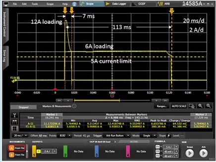
Figure 1: Example OCP system response time vs. overdrive
level
Here in Figure 1 the response time of the OCP system of a
Keysight N7951A 20V, 50A power supply was characterized using the companion
14585A software. It compares response times of 6A and 12A loading when the
current limit is set to 5A. Including the programmed OCP delay time of 5
milliseconds it was found that the actual total response time was 7
milliseconds for 12A loading and 113 milliseconds for 6A loading. As can be seen, for reasons previously
explained, the response time clearly depends on the amount of overdrive beyond
the current limit setting.
As the time to cause over current damage depends on the
amount of current in excess of what the DUT can tolerate, with greater current
causing damage more quickly, the slower response at lower overloads is
generally not an issue. If however you
are still looking how you might further improve on OCP response speed for more
effective protection, there are some things that you can do.
The first thing that can be done is to avoid using a
power supply that has a full output current rating that is far greater than
what the DUT actually draws. In this way the overdrive from an overload will be
a greater percentage of the full output current rating. This will normally
cause the current limit circuit to respond more quickly.
A second thing that can be done is to evaluate different
models of power supplies to determine how quickly their various current limit
circuits and OCP systems respond in based on your desired needs for protecting
your DUT. For various reasons different models of power supplies will have
different response times. As previously discussed in my first part, the slow
response at low levels of overdrive is determined by the response of the
current limit circuit.
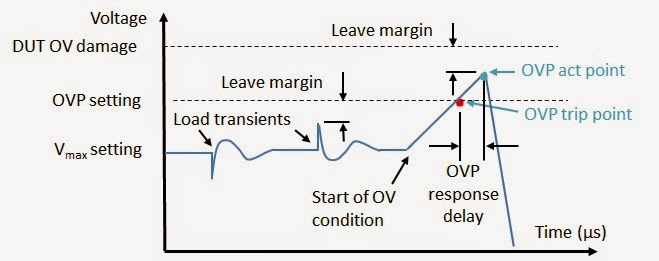
One more alternative that can provide exceptionally fast
response time is to have an OCP system that operates independently of a current
limit circuit, much like how an over voltage protect (OVP) system works. Here
the output level is simply compared against the protect level and, once
exceeded, the power supply output is shut down to provide near-instantaneous
protection. The problem here is this is not available on virtually any DC power
supplies and would normally require building custom hardware that senses the fault
condition and locally disconnects the output of the power supply from the DUT.
However, one instance where it is possible to provide this kind of
near-instantaneous over current protection is through the programmable signal
routing system (i.e. programmable trigger system) in the Keysight N6900A and
N7900A Advanced Power System (APS) DC power supplies. Configuring this
triggering is illustrated in Figure 2.

Figure 2: Configuring a fast-acting OCP for the
N6900A/N7900A Advanced Power System
In Figure 2 the N7909A software utility was used to
graphically configure and download a fast-acting OCP level trigger into an
N7951A Advanced Power System. Although this trigger is software defined it runs
locally within the N7951A’s firmware at hardware speeds. The N7909A SW utility
also generates the SCPI command set which can be incorporated into a test
program.
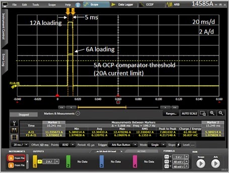
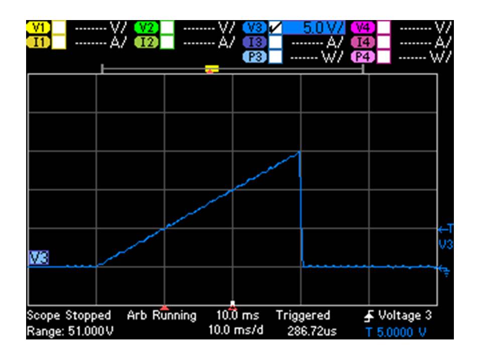
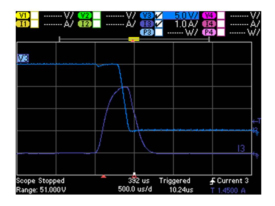
Figure 3: Example custom-configured OCP system response
time vs. overdrive level
Figure 3 captures the performance of this
custom-configured OCP system running within the N7951A. As the OCP
threshold and overdrive levels are the same this can be directly compared to
the performance shown in Figure 1, using the conventional, current limit based
OCP within the N7951A. A 5 millisecond OCP delay was included, as before.
However, unlike before, there is now virtually no extra delay due to a current
limit control circuit as the custom-configured OCP system is totally
independent of it. Also, unlike before, it can now be seen the same fast
response is achieved regardless of having just a small amount or a large amount
of overdrive.