Showing posts with label electronic load. Show all posts

Friday, August 14, 2015

Not all two-quadrant power supplies are the same when operating near or at zero volts!

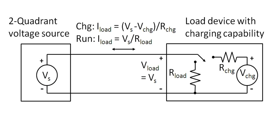
Occasionally when working with customers on power supply applications that require sourcing and sinking current which can be addressed with the proper choice of a two-quadrant power supply, I am told “we need a four-quadrant power supply to do this!” I ask why and it is explained to me that they want to sink current down near or at zero volts and it requires 4-quadrant operation to work. The reasoning why is the case is illustrated in Figure 1.


 Figure 1: Power supply sinking current while regulating near or at zero volts at the DUT

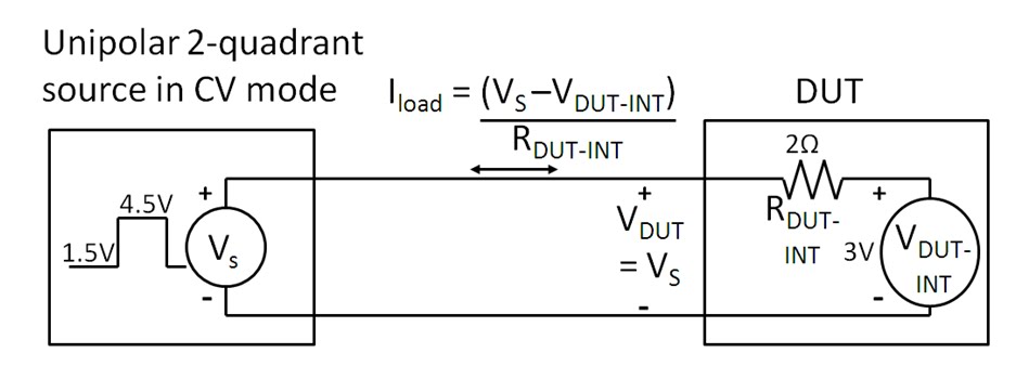
As can be seen in the diagram, in practical applications when regulating a voltage at the DUT when sinking current, the voltage at the power supply’s output terminals will be lower than the voltage at the DUT, due to voltage drops in the wiring and connections. Often this means the power supply’s output voltage at its terminals will be negative in order to regulate the voltage at the DUT near or at zero volts.

Hence a four-quadrant power supply is required, right? Well, not necessarily. It all depends on the choice of the two-quadrant power supply as they’re not all the same! Some two-quadrant power supplies will regulate right down to zero volts even when sinking current, while others will not. This can be ascertained from reviewing their output characteristics.

Our N6781A, N6782A, N6785A and N6786A are examples of some of our two-quadrant power supplies that will regulate down to zero volts even when sinking current.  This is reflected in the graph of their output characteristics, shown in Figure 2.


Figure 2: Keysight N6781A, N6782A, N6785A and N6786A 2-quadrant output characteristics

What can be seen in Figure 2 is that these two-quadrant power supplies can source and sink their full output current rating, even along the horizontal zero volt axis of their V-I output characteristic plots. The reason why they are able to do this is because internally they do incorporate a negative voltage power rail that allows them to regulate at zero volts even when sinking current. While you cannot program a negative output voltage on them, making them two-quadrants instead of four, they are actually able to drive their output terminals negative by a small amount, if necessary. This will allow them to compensate for remote sense voltage drop in the wiring, in order to maintain zero volts at the DUT while sinking current. This also makes for a more complicated and more expensive design.

Our N6900A and N7900A series advanced power sources (APS) also have two-quadrant outputs. Their output characteristic is shown in Figure 3.


Figure 3: Keysight N6900A and N7900A series 2-quadrant output characteristics

Here, in comparison, a certain amount of minimum positive voltage is required when sinking current. It can be seen this minimum positive voltage is proportional to the amount of sink current as indicated by the sloping line that starts a small maximum voltage when at maximum sink current and tapers to zero volts at zero sink current.  Basically these series of 2-quadrant power supplies are not able to regulate down to zero volts when sinking current. The reason why is because they do not have an internal negative power voltage rail that is needed for regulating at zero volts when sinking current.


So when needing to source and sink current and power near or at zero volts do not immediately assume a 4-quadrant power supply is required. Depending on the design of a 2-quadrant power supply, it may meet the requirements, as not all 2-quadrant power supplies are the same! One way to tell is to look at its output characteristics.

Monday, February 9, 2015

Consider using an electronic load for generating fast, high-power current pulses

Often there is the need for generating high-power current pulses, typically of short duration, and having rise and fall times on the order of microseconds. This is a common need when testing many types of power semiconductors, for example.

When looking for a DC power supply capable of generating very fast, high-power current pulses, one will find there are not a lot of options readily available that are capable of addressing their needs. There are specialized products dedicated for specific applications like this; an example of this is Keysight’s B1505A purpose-built semiconductor test equipment. They are capable of generating extremely fast, high-power current pulses.

Apart from specialized products however, DC power supplies generally to not offer this kind of speed when operating in a constant current mode (or current priority mode). One exception that comes to mind that we provide is our N6782A and N6782A DC source measure modules. They can create fast current pulses having just a couple of microseconds of rise and fall time. However, they are limited to 20V, 3A, and 20W of output. Most of the higher power, more general-purpose DC sources are not able to generate these kinds of fast, high-power current pulses and most are really more optimized to operate as voltage sources.

One alternative to consider for generating fast, high-power current pulses when working with general-purpose test equipment is to use an electronic load. You may initially say to yourself “an electronic load is for drawing pulses of current, not sourcing them!” but when coupled to a standard DC power supply operating as a voltage source, the setup is able to source fast, high-power current pulses. Most electronic loads are designed to have very fast current response. To illustrate this, I helped one customer needing to test their high brightness LED (HBLED) arrays with fast pulses of current. This was accomplished with the setup shown in Figure 1.


Figure 1: Load setup generating fast, high power current pulses for LED array testing

In this setup the power supply operates as a fixed, static voltage source. The power supply’s output voltage is set to the combined total of the full voltage needed to drive the HBLED array at full current plus the minimum voltage needed for the electronic load. The minimum voltage required for the electronic load is when it conducting maximum current and most of the power supply voltage is then applied across the HBLED array. The electronic load’s required minimum voltage is that which supports its operation in its linear range and maintains full dynamic response characteristics. In the case of Keysight electronic loads this minimum voltage for linear dynamic operation is 3 volts.  Conversely the maximum voltage required for the electronic load is when it drops down to minimum current level, where the power supply’s voltage is instead now being dropped across the electronic load instead of the HBLED array. Note that the electronic load may need to maintain a very small amount of bleed current to maintain linear operation in order to provide truly fast rise and fall times. In this way the electronic load is able to regulate the current across the full range with excellent dynamic response. This can be seen in Figure 2 where we were able to achieve approximately 15 microsecond rise time right from the start.


Figure 2: Pulsed current rise time in HBLED array

One advantage of this setup is the wide range of voltage and power that can be furnished to the DUT using a relatively low power electronic load. A common characteristic of electronic loads is that they can dissipate a given amount of power over an extended range of current and voltage. When the electronic load is at maximum current it is at minimum voltage. Conversely when it is near or at zero current it is then at its maximum voltage. In both cases there is only a small amount of power that the electronic load needs to dissipate. For an HBLED array it does not conduct a lot of current until it reaches about 75% of its full operating voltage. As a result the electronic load does not see a lot of power even on a transient basis. For this particular situation we chose to use the Keysight N3303A 240V, 10A, 250W electronic load. This gave a wide range of voltage, current, and power for testing a comparably wide range of different HBLED array assemblies.

So next time you need to source fast, high-power current pulses, you may want to think “load” instead of “source”!


Tuesday, December 30, 2014

Why does an electronic load draw a pulse of current when a voltage is initially applied?

We recently had a customer contact us about one of our electronic loads. He had a solid state switch in series with a fixed output voltage source (for example, 50 V) and set the load to a fixed current (for example, 1 A). He used a current probe and a scope to observe the current flowing into the electronic load. When the switch changed from open to closed he saw a pulse of current flowing into the load that was significantly higher than the load set value before the load settled to the set value of 1 A. He was wondering if this was normal. It is normal. Here’s why:

The electronic loads have a snubber network across their input terminals. The snubber typically consists of a resistor in series with a capacitor. For example, the Keysight N3304A electronic load has 2.2 uF in series with about 2 ohms. The snubber network is there to maintain stability on the load input for all settings and operating modes. When the customer’s switch was closed, the initially discharged capacitor in the snubber pulled a pulse of current to begin charging. If the dV/dt of the load input voltage waveform was infinitely fast, the cap would initially look like a short and the initial current pulse would be limited by the resistor as I = V/R. In this example, the current pulse would have been 50 V / 2 ohms = 25 A. But he was seeing a much smaller current pulse: around 2.4 A instead of 25 A, but still higher than the expected set value of 1 A. This means the dV/dt was not infinite (the solid state switch had a finite risetime). In this case, the current pulse would be limited by the dV/dt of the input voltage waveform.

As an example, see Figure 1 below showing the input voltage and input current for an N3304A load. The voltage rises from 0 V to 50 V over about 75 us and the fastest part of the risetime is about 1V/us. Since I = C dV/dt, and for this electronic load, C = 2.2 uF, the peak of the current is calculated to be 2.2 uF x 1V/us = 2.2 A. The plot shows it to be about 2.4 A, so this is close to the expected peak value. As the dV/dt of the input voltage slows down, the current drops from its peak and approaches zero amps as the dV/dt slows to zero (horizontal). (Note that in the plot below, the load was set for zero current.)

So you can see that the current flowing into the input of an electronic load may not be simply the DC setting you expect. If you apply a dynamic voltage waveform to the input, the RC snubber network will also draw some current for a short time until the voltage applied to the load input stabilizes. There is another factor involved here that is worth mentioning but I will not cover in detail in this post since it is a secondary effect in this case. In this customer’s situation, the load was set for 1 A and initially had no voltage on it (his solid state switch was open). The load was trying to draw current by turning on its input FETs, but there was no voltage applied, so the load went to an unregulated state. When the voltage finally appeared (the solid state switch was closed), the FETs that were turned on hard had to recover and take a finite amount of time to begin regulating the set current. This effect can also contribute to brief, temporary unexpected current draw by the load when a voltage is suddenly applied to the input.

Wednesday, August 20, 2014

Some differences between constant current (CC) and constant resistance (CR) loading on your DUT’s performance

Most electronic loads provide constant current (CC), constant resistance (CR) and constant voltage (CV) loading. Some also offer constant power (CP) loading as well. The primary reason for this is this gives the test engineer a choice of loading that best addresses the loading requirement for the DUT, which invariably is some kind of power source.

Most usually the device should be tested with a load that reflects what the loading is like for its end use. In the most common case of a device being predominantly a voltage source the most common loading choices are either CC or CR loading, which we will look at in more detail here. Some feel they can be used interchangeably when testing a voltage source. To some extent this is true but in some cases only one or the other should be used as they can impact the DUT’s performance quite differently.

Let’s first consider static performance. In Figure 1 we have the output characteristics of an ideal voltage source with zero output resistance (a regulated power supply, for example) and a non-ideal voltage source having series output resistance (a battery, for example).  Both have the same open circuit (no load) voltage. Superimposed on these two source output characteristics are two load lines; one for CC and one for CR. As can be seen they are set to draw the same amount of current for the ideal voltage source. However, for the non-ideal voltage source, while the CC load still continues to draw the same amount of current in spite of the voltage drop, not surprisingly the CR load draws less current due to its voltage-dependent nature.


Figure 1: CC and CR loading of ideal and non-ideal voltage sources

CC loading is frequently used for static power supply tests for a key reason. Power supplies are usually specified to have certain output voltage accuracy for a fixed level of current. Using CC loading assures the loading condition is met, regardless of power supply’s output voltage being low or high, or in or out of spec. Non-ideal voltage sources, like batteries, present a little more of a problem and are often specified for both CC and CR loading as a result, to reflect the nature of the loading they may be subjected to in their end use. Due to a battery's load-dependent output voltage, trying to use one type of loading in place the other becomes an iterative process of checking and adjusting loading until the acceptable operating point is established.

Let’s now consider dynamic performance.  CC loading generally has a greater impact on a power supply’s ability to turn on as well as its transient performance and stability, in comparison to CR loading. When the power supply first starts up its output voltage is at zero. A CR load would demand zero current at start up. In comparison a CC load still demands full current. Some power supplies will not start up properly under CC loading. With regard to transient response and stability, CR loading provides a damping action, increasing current demand when the transient voltage increases and decreases demand when the transient voltage decreases, because the current demand is voltage dependent. CC loading does not do this, which can negatively influence transient response and stability somewhat. Whether CC or CR loading is used depends on what the power supply’s specifications call out for the test conditions. Batteries have some dynamic considerations as well. Their output response can be modeled as a series of time constants spanning a wide range of time. This presents somewhat of a moving target for an algorithm that uses an iterative approach to settling on an acceptable operating point.


This is just a couple of examples of how a load’s characteristic affects the performance of the device it is loading, and why electronic loads have multiple operating modes to select from, and worth giving thought next time towards how your device is affected by its loading!

Tuesday, June 3, 2014

Upcoming Webinar on High Power Source/Sink Solutions for Testing Bidirectional Energy Devices

Bidirectional and regenerative energy devices both source and sink power and energy. Correspondingly, a solution that can both source and sink power and energy is needed for properly testing them. In the past here on “Watt’s up?” we have talked about what two and four quadrant operation is in our posting “What is bipolar four quadrant power? (Click here to review). We have also talked about cross over behavior between sourcing and sinking current with a DC source that will operate in two quadrants in a two-part posting  “Power supply current source-to-sink crossover characteristics” (Click here to review pt. 1) and (Click here to review pt. 2). These give useful insights about the nature of multi-quadrant solutions for bi-directional test applications.


Figure 1: The four operating quadrants

Bidirectional and regenerative energy devices that are used in many applications, such as satellite power systems, alternative energy, automotive, and many other areas, operate at kilowatt and higher power levels. These higher power levels have a significant impact on solutions and approaches taken to address their testing.  Also, the nature of these bidirectional and regenerative energy devices are not all the same. This also has an impact in that the capabilities of the test solutions need to be different to address these different types of devices.

In my upcoming webinar on June 18th, titled “Conquering the High Power Source/Sink Test Challenge” I will be exploring the test needs of key bidirectional and regenerative energy devices and then go into the details of various test solutions and approaches for sourcing and sinking power and energy, along with their associated advantages and disadvantages. This is just a couple of weeks away. So if you are involved in this kind of work and are interested, or would just like to learn more, you can register online at the following (click here).  In case you cannot join the live event you will still be able to register and listen to seminar afterward instead, as it will be recorded.  I hope you can join in!


.

Monday, February 24, 2014

How to test the efficiency of DC to DC converters, part 2 of 2

In part 1 of my posting on testing the efficiency of DC to DC converters (click here to review) I went over the test set up, the requirements for load sweep synchronized to the measurements, and details of the choice of the type and set up of the current load sweep itself. In this second part I will be describing details of the measurement set up, setting up the efficiency calculation, and results of the testing. This is based on using the N6705B DC Power Analyzer, N6782A SMUs, and 14585A software as a platform but a number of ideas can be applicable regardless of the platform.


Figure 1: Synchronized measurement and efficiency calculation set up

The synchronized measurement and efficiency calculation set up, and display of results are shown in Figure 1, taking note of the following details corresponding to the numbers in Figure 1:
  1. In the 14585A the data logging mode was selected to make and display the measurements. The oscilloscope mode could have just as easily been used but with a 10 second sweep the extra speed of sampling with the oscilloscope mode was not an advantage. A second thing about using the data logging mode is you can set the integration time period for each acquisition point. This can be used to advantage in averaging out noise and disturbances as needed for a smoother and more representative result. In this case an integration period of 50 milliseconds was used.
  2. To synchronize the measurements the data log measurement was set to trigger off the start of the load current sweep.
  3. Voltage, current, and power for both the input and output SMUs were selected to be measured and displayed. The input and output power are needed for the efficiency calculation.
  4. The measurements were set to seamless ranging. In this way the appropriate measurement range for at any given point was used as the loading swept from zero to full load.
  5. A formula trace was created to calculate and display the efficiency in %. Note that the negative of the ratio of output power to input power was used. This is because the SMU acting as a load is sinking current and so both its current and power readings are negative.


With all of this completed really all that is left to do is first start the data logging measurement with the start button. It will be “armed” and waiting from a trigger signal from the current load sweep ARB that had been set up. All that is now left to do is press the ARB start button. Figure 2 is a display of all the results after the sweep is completed.


Figure 2: DC to DC Converter efficiency test results

All the input and output voltage, current, and power measurements, and efficiency calculation (in pink) are display, but it can be uncluttered a bit by turning off the voltages and currents traces being displayed and just leave the power and efficiency traces displayed. This happened to be special DC to DC converter designed to give exceptionally high efficiency even down to near zero load, which can be seen from the graph. It’s interesting to note peak efficiency occurred at around 60% of full load and then ohmic losses start becoming more significant.

And that basically sums it all up for performing an efficiency test on a DC to DC converter!

Thursday, February 20, 2014

How to test the efficiency of DC to DC converters, part 1 of 2

I periodically get asked to provide recommendations and guidance on testing the efficiency of small DC to DC voltage converters. Regardless of the size of the converter, a DC source is needed to provide input power to the converter under constant voltage, while an electronic load is needed to draw power from the output, usually under constant current loading. The load current needs to be swept from zero to the full load current capability of the DC to DC converter while input power (input voltage times input current) and output power (output voltage times output current) are recorded. The efficiency is then the ratio of power out to power in, most often expressed in a percentage. An illustration of this is shown in Figure 1. In addition to sourcing and sinking power, precision current and voltage measurement on both the input and output, synchronized to the sweeping of the load current is needed.


Figure 1: DC to DC converter efficiency test set up

One challenge for small DC to DC voltage converters is finding a suitable electronic load that will operate at the low output voltages and down to zero load currents, needed for testing their efficiency over their range, from no load to full load output power. It turns out in practice many source measure units (SMUs) will serve well as a DC electronic load for testing, as they will sink current as well as source current.

Perhaps the most optimum choice from us is to use two of our N6782A 2-quadrant SMU modules installed in our N6705B DC Power Analyzer mainframe, using the 14585A software to control the set up and display the results.  This is a rather flexible platform intended for a variety of whatever application one can come up with for the most part. With a little ingenuity it can be quickly configured to perform an efficiency test of small DC to DC converters, swept from no load to full load operation. This is good for converters of 20 watts of power or less and within a certain range of voltage, as the N6782A can source or sink up to 6 V and 3 A or 20 V and 1 A, depending on which range it is set to. One of the N6782A operates as a DC voltage source to power the DUT and the second is operated as a DC current load to draw power from the DUT. A nice thing about the N6782A is it provides excellent performance operated either as a DC source or load, and operated either in constant voltage or constant current.

An excellent video of this set up testing a DC to DC converter was created by a colleague here, which you can review by clicking on the following link: “DC to DC converter efficiency test”.

The video does an excellent job covering a lot of the details. However, if you are interested in testing DC to DC converters using this set up I have a few more details to share here about it which should help you further along with setting it up and running it.

First, the two N6782A SMUs were set up for initial operating conditions. The N6782A providing DC power in was set up as a voltage source at the desired input voltage level and the second N6782A was set to constant current load operation with minimum (near zero) loading current.

Note that the 14585A software does not directly sweep the load current along the horizontal axis. The horizontal axis is time. That is why a time-based current sweep was created in the arbitrary waveform (ARB) section of the 14585A. In that way any point on the horizontal time axis correlates to a certain current load level being drawn from the output of the DUT. The ARB of course was set to run once, not repetitively. The 14585A ARB set up is shown in Figure 2.


Figure 2: Load current sweep ARB set up in 14585A software

This ARB sweep requires a little explanation.  While there are a number of pre-defined ARBs, and they can be used, an x3 power formula was chosen to be used instead. This provided a gradually increasing load sweep that allowed greater resolution of this data and display at light loads, where efficiency more quickly changes. As can be seen, the duration of the sweep, parameter x, was set to 10 seconds. As a full load current needed to be -1 A, using the actual formula (-x/10)3  gave us a gradually increasing load current sweep that topped out at -1A after 10 seconds of duration. The choice of 10 seconds was arbitrary. It only provided an easy way to watch the sweep on the 14585A graphing as it progressed. Finally, a short (0.1 second) pre-defined linear ramp ARB was added as a second part of the ARB sequence, to bring the load current back to initial, near zero, load conditions after the sweep was completed. This is shown in Figure 3.


Figure 3: Second part of ARB sweep to bring DUT load current back to initial conditions


I hope this gives you a number of insights about creative ways you can make use of the ARB. As there is a good amount of subtle details on how to go about making and displaying the measurements I’ll be sharing that in a second part coming up shortly, so keep on the outlook!

Friday, January 24, 2014

Using Binary Data Transfers to Improve Your Test Throughput

From time to time I have shared here on “Watt’s Up?” a number of different ways the system DC power supply in your test set up impacts your test time, and recommendations on how to make significant improvements in the test throughput. Many of these previous posts are based on the first five of ten hints I’ve put together in a compendium entitled “10 Hints on Improving Throughput with your Power Supply” (click here for hints 1-5).

Oscilloscopes, data acquisition, and a variety of other test equipment are often used to capture and digitize waveforms and store large arrays of data during test, the data is then downloaded to a PC. These data arrays can be quite large, from thousands to millions of measurements. For long-term data logging the data files can be many gigabytes in size. These data files can take considerable time to transfer over an instrument bus, greatly impacting your test time.

Advanced system power supplies incorporating digitizing measurement systems to capture waveform measurements like inrush current are no different. This includes a number of system DC and AC power products we provide. Even though you usually have the choice of transferring data in ASCII format, one thing we recommend is instead transfer data in binary format. Binary data transmission requires fewer bytes reducing transfer time by a factor of two or more.


Further details about using binary mode data transfers can be found in hint 7 of another, earlier compendium we did, entitled “10 hints for using your power supply to decrease test time” (click here to access). Between these two compendiums of hints for improving your test throughput I expect you should be able find a few different ideas that will benefit your particular test situation!

Wednesday, November 27, 2013

Why can’t you put electronic loads in series?

The quick answer to the above question is: because you will likely damage at least one of the loads with excessive voltage! For the longer answer, read on….

[By the way…this is a milestone post for Watt’s Up? since it is post # 100, so thank you to our readers…and Happy Thanksgiving to those in the US or celebrating elsewhere!]

I’ll start with a brief explanation of what an electronic load is, and what it is used for. I am specifically talking about DC electronic loads here. A DC electronic load is a two-terminal electrical instrument that draws power from a DC source. Loads are used to test DC sources. Any device that has a source of DC output power, such as a DC power supply, a DC-to-DC converter, a battery, a fuel cell, or a solar panel, can have power drawn from it with an electronic load. Click here to see Agilent’s DC electronic loads.


For example, to test a fixed-output DC power supply that is rated for 20 V, 5 A, 100 W, you would connect the power supply output to an electronic load with ratings that are equal to or greater than the power supply ratings and that can draw a constant current from the power supply. Since the power supply is regulating the voltage (20 V), the load must regulate the current it draws from the power supply (up to 5 A). If your DC power supply is a constant current source, the load must be capable of drawing power while regulating voltage. You can set most electronic loads to draw power by regulating either constant voltage (CV) or constant current (CC). You can also set many electronic loads to regulate constant resistance (CR) across their input terminals, and some can regulate constant power (CP).

If the power supply to be tested has a higher output voltage than a single electronic load can handle, you may be tempted to put multiple load inputs in series to accommodate the higher voltage. After all, you can do this will power supply outputs to get higher voltage (click here)….why not with loads?

Putting electronic loads in series can cause one of the load inputs to be exposed to a voltage beyond its capabilities that could result in damage to the load. You are putting loads in series because a single load does not have a high enough voltage rating to handle the voltage of your DC power source. But since one of the load inputs could become a low impedance (nearly a short circuit) during test, all of the voltage from your DC source could appear across the other load input in series. There are several scenarios that can result in this destructive situation. To understand these scenarios, you first have to understand how an electronic load works.

Loads work by controlling the conduction of FETs across their input terminals. The control is realized by using a feedback loop to adjust a measured level (such as the input current) so that it equals a reference level (such as the set current). My colleague, Ed Brorein, posted about this topic last year (click here).

When you put multiple electronic loads in series to accommodate higher voltage, one problem scenario occurs when you set both loads to operate in CC mode. You set the same current on both loads. The exact same current flows through both loads (see figure below), but due to small errors in the accuracy of the settings, the real set values will never be exactly equal. Therefore, one of the loads will be trying to draw a higher current (Load 2 in the figure) than the other load (Load 1 in the figure). Since Load 1 will limit the current at the lower value (9.99 A in this example), Load 2 can never attain its real set point (10.01 A in this example). So its internal feedback loop continues to tell the FETs to conduct more and more current until the FETs are fully on looking nearly like a short circuit. This results in nearly all of the power supply voltage appearing across the Load 1 input which can damage it.


If you operate one load input in CC and one in CV, at first this looks like it will result in a stable operating point. However you have to think about how you get to that stable operating point. If you set the loads first before you connect the voltage, before the voltage is applied, the CC load is not satisfied (no current is flowing) so it goes to a short and the CV load is also not satisfied (no voltage is present) so it goes to an open. When the test voltage is applied, all of the voltage initially appears across the open CV load and can damage it. There are other procedures to follow that could temporarily result in a stable operating point (such as slowly increasing the test voltage if you have that ability), but if any fault condition occurs in any of the loads, they try to protect themselves by either turning the FETs on hard (a short) or opening the FETs. In either case, the large destructive voltage will appear across one of the loads in the series connection resulting in damage.

One of my colleagues, Bob Zollo, wrote an article entitled “Why Can’t You Put Electronic Loads In Series To Get More Voltage?” that appeared in Electronic Design on November 4, 2013. For some additional information about this topic, click here to read the article.

So you can see that putting loads in series can too easily result in damage to at least one of the load inputs. I strongly recommend that you do not do it!

Thursday, June 20, 2013

How can I measure output impedance of a DC power supply?

In my last posting “DC power supply output impedance characteristics”, I explained what the output impedance characteristics of a DC power supply were like for both its constant voltage (CV) and constant current (CC) modes of operation. I also shared an example of what power supply output impedance is useful for. But how does one go about measuring the output impedance of a DC power supply over frequency, if and when needed?

There are a number of different approaches that can be taken, but these days perhaps the most practical is to use a good network analyzer that will operate at low frequencies, ranging from 10 Hz up to 1 MHz, or greater, depending on your needs. Even when using a network analyzer as your starting point there are still quite a few different variations that can be taken.

Measuring the output impedance requires injecting a disturbance at the particular frequency the network analyzer is measuring at. This signal is furnished by the network analyzer but virtually always needs some amount of transformation to be useful. Measuring the output impedance of a voltage source favors driving a current signal disturbance into the output. Conversely, measuring the output impedance of a current source favors driving a voltage signal disturbance into the output. The two set up examples later on here use two different methods for injecting the disturbance.

The reference input “R” of the network analyzer is then used to measure the current while the second input “A” or “T” is used to measure the voltage on the output of the power supply being characterized. Thus the relative gain being measured by the network analyzer is the impedance, based on:
zout = vout/iout = (A or T)/R
The output voltage and current signals need to be compatible with the measurement inputs on the network analyzer. This means a voltage divider probe may be needed for the voltage measurement, depending on the voltage level, and a resistor or current probe will be needed to convert the current into an appropriate voltage signal. A key consideration here is appropriate scaling constants need to be factored in, based on the gain or attenuation of the voltage and current probes being used, so that the impedance reading is correct.


Figure 1: DC power supply output impedance measurement with the Agilent E5061B

One example set up using the Agilent E5061B network analyzer is shown in Figure 1, taken from page 15 of an Agilent E5061B application note on testing DC-DC converters, referenced below. Here the disturbance is injected in through an isolation transformer coupled across the power supply output through a DC blocking capacitor and a 1 ohm resistor. The 1 ohm resistor is doing double duty in that it is changing the voltage disturbance into a current disturbance and it is also providing a means for the “R” input to measure the current. The “T” input then directly measures the DC/DC converter’s (or power supply’s) output voltage.

A second, somewhat more elaborate, variation of this arrangement, based on using a 4395A network analyzer (now discontinued) has been posted by a colleague here on our Agilent Power Supply forum: “Output Impedance Measurement on Agilent Power Supplies”. In this set up the disturbance signal from the network analyzer is instead fed into the analog input of an Agilent N3306A electronic load. The N3306A in turn creates the current disturbance on the output of the DC power supply under test as well as provide any desired DC loading on the power supply’s output. The N3306A can be used to further boost the level of disturbance if needed. Finally, an N278xB active current probe and matching N2779A probe amplifier are used to easily measure the current signal.

Hopefully this will get you on your way if the need for making power supply output impedance ever arises!


Reference: “Evaluating DC-DC Converters and PDN with the E5061B LF-RF Network Analyzer” Application Note, publication number 5990-5902EN (click here to access)

Friday, January 18, 2013

Types of current limits for over-current protection on DC power supplies


On a previous posting “The difference between constant current and current limit in DC power supplies”, I discussed what differentiates a DC power supply having a constant current operation in comparison to having strictly a current limit for over-current protection. In that post I had depicted one very conventional current limit behavior. However there is actually quite a variety of current limits incorporated in different DC power supplies, depending on the intended end-use of the power supply.

Fold-back Current Limit
The output characteristic of a constant voltage (CV) power supply utilizing fold-back current limiting is depicted in Figure 1. Fold-back current limiting is sometimes used to provide a higher level of protection for DUTs where excess current and power dissipation can cause damage to a DUT that has gone into an overload condition. This is accomplished by reducing both the current and voltage as the DUT goes further into overload. The short circuit current will typically be 20% to 50% of the maximum current level. A reasonable margin between the crossover current point and required maximum rated DUT current needs to be established in order to prevent false over-current tripping conditions. Due to the fold-back nature, and depending on the loading nature of the DUT, the operating point could drop down towards the short-circuit operating point once the crossover point is reached/exceeded. This would require powering the DUT down and up again in order to get back to the CV operating region.


Figure 1: Output characteristic of a CV power supply with fold-back current limiting

In addition to providing over-current protection for the DUT, fold-back current limiting is often employed in fixed output linear DC power supplies as a means for reducing worst case dissipation in the power supply itself. Under short circuit conditions the voltage normally appearing across the DUT instead appears across the power supply’s internal series linear regulator, requiring it to dissipate considerably more power than it has to under normal operating conditions. By employing fold-back current limiting the power dissipation on the series-linear regulator is greatly reduced under overload conditions, reducing the size and cost of the series-linear regulator for a given output power rating of the DC linear power supply.


Fold-forward Current Limit
A variety of loading devices, such as electric motors, DC-DC converters, and large capacitive loads can draw large peak currents at startup. Because of this they can often be better suited for being powered by a DC power supply that has a fold-forward current limit characteristic, as depicted in Figure 2. With fold-forward current limiting after exceeding the crossover current limit the current level instead continues to increase while the voltage drops while the loading increases.


Figure 2: Output characteristic of a CV power supply with fold-forward current limiting

As one example of where fold-forward current limiting is a benefit, it can help a motor start under load which otherwise would not start under other current-limits. Indeed, with fold-back current limiting, a motor may not and then it would remain stalled, due to the reduced current.

Special Purpose Current Limits
Unlike the previous current limit schemes which are widely standard practice, there is a number of other current limit circuits used, often tailored for more application-specific purposes. One example of this is the current limiting employed in our 66300 series DC sources for powering mobile phones and other battery powered mobile wireless devices. Its output characteristic is depicted in Figure 3.


Figure 3: Agilent 66300 Series DC source output characteristics

We refer to this power supply series as battery emulator DC sources. One reason why is they are 2-quadrant DC sources.  Like a rechargeable battery, they need to be able to source current when powering the mobile device and then sink current when the mobile device is in its charging mode.  In Figure 3 there are actually two separate current limits; one for sourcing current and another for sinking current. Each has different and distinctive characteristics for specific purposes.

Many battery powered mobile wireless devices draw power and current in short, high peak bursts, especially when transmitting. To better accommodate these short, high peaks, the 66300 series DC sources have a time-limited peak current limit that is of sufficient duration to support these high peaks. They also have a programmable constant current level that will over-ride the peak current limit when the average current value of the pulsed current drain reaches this programmed level. With this approach a higher peak power mobile device can be powered from a smaller DC power source.

Just like an electronic load, when the 66300 series DC source is sinking current the limiting factor is how much power it is able to dissipate. Instead of using a fixed current limit, it uses a fold-forward characteristic current limit (although folding forward in the negative direction!). This is not done for reasons that a fold-forward current limit that was just discussed is used; it is done so higher charging currents at lower voltage levels can be accommodated, taking advantage of the available power that can be dissipated. Again, this provides the user with greater capability in comparison to using a fixed-value limit.

Other types of current limits exist for other specific reasons so it is helpful to be aware that not all current limits are the same when selecting a DC power supply for a particular application!

Reference: Agilent Technologies DC Power Supply Handbook, application note AN-90B, part number 5952-4020 “Click here to access”

Monday, December 10, 2012

More on power supply current source-to-sink crossover characteristics


On my earlier posting “Power supply current source-to-sink crossover characteristics” I showed what the effects on the output voltage of a unipolar two-quadrant-power supply were, resulting from the output current on the power supply transitioning between sourcing and sinking. In that example scenario, the power supply was maintaining a constant output voltage and the transitioning between sourcing and sinking current was dictated by the external device connected to and being powered by the power supply. This is perhaps the most common scenario one will encounter that will drive the power supply between sourcing current and sinking current.

Other scenarios do exist that will drive a unipolar two-quadrant power supply to transition between sourcing and sinking output current. One scenario is nearly identical to the earlier posting. However, instead of the device transitioning its voltage between being less and greater than the power supply powering it, the power supply instead transitions its voltage between being less and greater than the active device being normally powered.  A set up for evaluating this scenario on an Agilent N6781A two-quadrant DC source is depicted in Figure 1.


Figure 1: Evaluating current source-to-sink crossover on an N6781A operating in constant voltage

In this scenario having the DC source operating as a voltage source and transitioning between 1.5 and 4.5 volts causes the current to transition between -0.75 and +0.75A.  The voltage and current waveforms captured on an oscilloscope are shown in Figure 2.


Figure 2: Voltage and current waveforms for the set up in Figure 1

The waveforms in Figure 2 are as what should be expected. The actual transition points are where the current waveform passes through zero on the rising and falling edge. An expanded view to the current source-to-sink transition is shown in Figure 3.


Figure 3: Expanded voltage and current waveforms for the set up in Figure 1

As can be seen the voltage ramp transitions smoothly at the threshold point, or zero crossing point, of the current waveform. The reason being is that the DC is maintaining its operation as a voltage source. Its voltage feedback loop is always in control.


Yet one more scenario that will drive a unipolar two-quadrant source to transition between sourcing and sinking current is operate it as a current source and program is current setting between positive and negative values. In this case the device under test that was used is a voltage source.  One real-world example is cycling a rechargeable battery by alternately applying charging and discharging currents to it. The set up for evaluating this scenario, again using an N6781A two-quadrant DC source is depicted in Figure 4.


Figure 4: Evaluating current source-to-sink crossover on an N6781A operating in constant current

For Figure 4 the N6781A was set to operate in constant current and programmed to alternately transition between -0.75A and +0.75A current settings. The resulting voltage and current waveforms are shown in Figure 5.


Figure 5: Voltage and current waveforms for the set up in Figure 4

The waveforms in Figure 5 are as what should be expected. The actual transition points are where the current waveform passes through zero on the rising and falling edge. An expanded view to the current source-to-sink transition is shown in Figure 6.


Figure 6: Expanded voltage and current waveforms for the set up in Figure 4

As the N6781A is operating in current priority the interest is in how well it controls its current while transitioning through the zero-crossing point. As observed in Figure 6 it transitions smoothly through the zero-crossing point. The voltage performance is determined by the DUT, not the N6781A, as the N6781A is operating in constant current.

So what was found here is, for a unipolar two-quadrant DC source, transitioning between sourcing and sinking current should generally be virtually seamless as, under normal circumstances, should remain in either constant voltage or constant current during the entire transition.

Wednesday, December 5, 2012

Power supply current source-to-sink crossover characteristics


A two-quadrant power supply is traditionally one that outputs unipolar voltage but is able to both source as well as sink current. For a positive polarity power source, when sourcing current it is operating in quadrant 1 as a conventional power source. When sinking current it is operating in quadrant 2 as an electronic load. Conversely, a negative polarity two-quadrant  power source operates in quadrants three and four. Further details on power supply operating quadrants are provided in a recent posting here in ‘Watt’s Up?”, What is a bipolar (four-quadrant) power supply? Often a number of questions come up when explaining two-quadrant power supply operation, including:
  • What does it take to get the power supply operating as a voltage source to cross over from sourcing to sinking current?
  • What effect does crossing over from sourcing to sinking current have on the power supply’s output?


For a two-quadrant voltage source to be able to operate in the second quadrant as an electronic load, the device it is normally powering must also be able to source current and power as well as normally draw current and power. Such an arrangement is depicted in Figure 1, where the device is normally a load, represented by a resistance, but also has a charging circuit, represented by a switch and a voltage source with current-limiting series resistance.


Figure 1: Voltage source and example load device arrangement for two-quadrant operation.

There is no particular control on a two-quadrant power supply that one has to change to get it to transition from sourcing current and power to sinking current and power from the device it is normally powering. It is simply when the source voltage is greater than the device’s voltage then the voltage source will be operating in quadrant one sourcing power and when the source voltage is less than the device’s voltage the voltage source will be operating in quadrant two as an electronic load. In figure 1, during charging the load device can source current back out of its input power terminals as long as the charger’s current-limited voltage is greater than the source voltage.

It is assumed that load device’s load and charge currents are lower than the positive and negative current limits of the voltage source so that the voltage source always remains in constant voltage (CV) operation. A step change in current is the most demanding from a transient standpoint, but as the voltage source is always in its constant voltage mode it handle the transition well as its voltage control amplifier is always in control. This is in stark contrast to a mode cross over between voltage and current where different control amplifiers need to exchange control of the power supply’s output. In this later case there can be a large transient while changing modes. See another posting, Why Does My Power Supply Overshoot at Current Limit? Insights on Mode Crossover” for further information on this.  There is a specification given on voltage sources which quantifies the impact one should expect to see from a step change in current going from sourcing current to sinking current, which is its transient voltage response.  A transient voltage response measurement was taken on an N6781A two-quadrant DC source, stepping the load from 0.1 amps to 1.5 amps, roughly 50% of its rated output current.


Figure 2: Agilent N6781A transient voltage response measurement for 0.1A to 1.5A load step

However, the transient voltage response shown in Figure 2 was just for sourcing current. With a well-designed two-quadrant voltage source the transient voltage response should be virtually unchanged for any step change in current load, as long as it falls within the voltage source’s current range.  The transient voltage response for an N6781A was again capture in Figure 3, but now for stepping the load between -0.7A and +0.7A.


Figure 3: Agilent N6781A transient voltage response measurement for -0.7A to +0.7A load step

As can be seen in Figures 2 and 3 the voltage transient response for the N6781A remained unchanged regardless of whether the stepped load current was all positive or swung between positive and negative (sourcing and sinking).

While the transient voltage response addresses the dynamic current loading on the voltage source there is another specification that addresses the static current loading characteristic, which is the DC load regulation or load effect.  This is a very small effect on the order of 0.01% output change for many voltage sources. For example, for the N6781A the load effect in its 6 volt range is 400 microvolts for any load change. In the case of the N6781A being tested here the DC change was the same for both the 0.1 to 1.5 amp step and the -0.7 to +0.7 amp step change.


There are two more scenarios which will cause a two-quadrant power supply transition between current sourcing and sinking.  The first is very similar to above with the two-quadrant power supply operating in constant voltage (CV) mode, but instead of the DUT changing, the power supply changes its voltage level instead.  The final scenario is having the two-quadrant power supply operating in constant current with the DUT being a suitable voltage source that is able to source and sink power as well, like a battery for example. Here the two-quadrant power supply can be programmed to change from a positive current setting to a negative current setting, thus transitioning between sourcing and sinking current again, and its current regulating performance is now a consideration.  Both good topics for future postings!

Thursday, November 15, 2012

Validating battery capacity under end-use conditions for battery powered mobile devices


One aspect (of many) I have talked about for optimizing battery life for battery powered mobile devices is assessing the battery’s actual capacity. Not only do you need to assess its capacity under conditions as stated by the manufacturer but also under conditions reflecting actual end use.

Validating the battery under a manufacturer’s stated conditions establish a starting point of what you might be achievable in how much capacity you can obtain from the battery and if it is in line with what the manufacturer states. Sometime it can be less for a variety of reasons. Even subtle differences in stated conditions can lead to fairly substantial differences in capacity. The stated conditions usually provide a “best case” achievable value for capacity. Do not be surprised if your results for the battery’s capacity fall a little short of the best case value provided by the manufacturer. With a little work you may be able to determine what subtle difference caused it, or simply, the best case value given is a bit optimistic.

Validating the battery under end-use conditions helps establish the difference you can expect between the battery’s capacity for rather ideal stated conditions against end-use conditions. Battery powered mobile devices draw current in a pulsed fashion, with high peaks in relation to the overall average current drain. An example of this kind of dynamic current drain is shown in Figure 1. In this case it is the active mode current drain of a GPRS smart mobile phone.


Figure 1: GPRS smart mobile phone dynamic current drain waveform

This usually significantly degrades the battery’s delivered capacity in comparison to the manufacturer’s stated conditions, which are based on a constant DC current discharge. If you do not take the impact of end-use loading conditions on the battery’s capacity into account there is a good chance the mobile device’s run-time will fall quite a bit short of expectations.

The usual way to validate a battery’s capacity under end-use conditions is to actually hook the battery together with its device, connect up logging instrumentation for recording the battery run down voltage and current over time, and then placing the device in a desired operating mode and let it run until the battery is run down. While a battery run-down test like this is useful to do it has a couple of issues when trying to focus explicitly on just the battery:
  • It is a test of the combination of the battery together with its host device. The host device also has influence on the test’s outcome and must be taken into account in assessing just the battery under end-use.
  • It can often be complex and difficult to set up the device in its desired operating condition, requiring a substantial amount of supporting equipment to recreate its environment for providing a realistic operating condition.
  • It can sometimes be difficult to get consistently repeatable results with the actual device.

An alternative to repeatedly using the actual device is to use an electronic load that can draw a dynamic current representative of the actual device the electronic load is being used in place of. In some cases a simple low duty cycle, high crest factor pulsed current waveform can be directly programmed into the electronic load. In cases where the host device’s current drain waveform is a bit more complex it may be useful to have an electronic load that is able to “play back” a digitized waveform file that is a representative portion of the device’s actual current drain, on an ongoing basis to run down the battery. As one example we put features into our 14585A software to simplify this record and playback approach using our N6781A 2-quadrant DC source measure module. This set up is depicted in Figure 2.


Figure 2: Current drain record and playback set up using the 14585 and N6781A

In the first half of this process the N6781A serves as a voltage source to power up the device while digitizing its dynamic current drain waveform. In the second half of this process the captured current drain waveform is inverted and then played back by the N6781A now instead operating as a constant current load connected to a battery to discharge it. A colleague in our office recently completed a video of how to do this record and playback process using a digital camera as an example, capturing the current drain waveform of the process of taking a picture. This could be played back repeatedly to determine how many pictures could be taken with a set of batteries, for example. I know with my digital camera I need to take a spare set of batteries with me as it uses up batteries quite quickly! The video is available to be viewed at the following link:“record and playback video”

Thursday, November 8, 2012

Configuring an Electronic Load for Zero Volt Operation


DC electronic loads are indispensable for testing a variety of DC power sources. There are a number of situations that call for testing DC power sources at low voltage, even right down to zero volts. Often this is also at relatively high current of many tens of amps or greater. Some examples include:
  • Low output voltage power supplies and DC/DC converters (mostly for digital circuit power)
  • Solar cell I-V testing, down to zero volts
  • Fuel cell testing
  • Single cell battery testing
  • Power supply true output short-circuit testing, down to zero volts


It becomes challenging for the test engineer to find adequate DC electronic loads for low voltage operation, especially at high currents. Many DC electronic loads, including the ones Agilent Technologies provides, use multiple power FETs for their input loading element. While a power FET can actually operate down to zero volts, this is at zero current as well. At high current a few volts is typically needed for stable, dynamic operation at full current.  As one example Figure 1 depicts the input I-V characteristics of an Agilent N3304A DC electronic load.


Figure 1: Agilent N3304A DC electronic load input I-V characteristics

An effective solution for low voltage electronic load operation, right down to zero volts, for the electronic load’s full rated current, is to connect a low voltage boost power supply in series with the electronic load’s input. An example of this set up is depicted in Figure 2.


Figure 2: Zero volt DC electronic load set up

The electronic load now sees the sum of the boost supply’s and DUT’s voltages. Selecting a boost supply having adequate voltage will assure the electronic load will be able to operate at full performance at full current, even when the voltage at the DUT is zero. There are a few things that need to be paid attention to:
  • The electronic load needs to dissipate the total power of both the boost supply and DUT
  • The DUT needs to be adequately safeguarded against reverse polarity if the electronic load is inadvertently turned on too hard
  • The electronic load’s voltage sensing must be able to accommodate the extra voltage difference between the electronic load and DUT, due to the boost supply voltage
  • The boost supply ripple and noise (PARD) can contribute to noise measurements made on the DUT


Due to these considerations not all electronic loads may be well suited for zero volt operation with a boost supply so it is necessary to validate if a particular electronic load under consideration can be applied in this manner first.  Further details about zero voltage load operation as well as using Agilent N3300 series DC electronic loads for this purpose are described in product note “Agilent Zero Volt Electronic Load”, publication number 5968-6360E. Click here to access

Tuesday, August 7, 2012

How Does an Electronic Load Regulate It’s Input Voltage, Current, and Resistance?


In a sense electronic loads are the antithesis of power supplies, i.e. they sink or absorb power while power supplies source power. In another sense they are very similar in the way they regulate constant voltage (CV) or constant current (CC). When used to load a DUT, which inevitably is some form of power source, conventional practice is to use CC loading for devices that are by nature voltage sources and conversely use CV loading for devices that are by nature current sources. However most all electronic loads also feature constant resistance (CR) operation as well. Many real-world loads are resistive by nature and hence it is often useful to test power sources meant to drive such devices with an electronic load operating in CR mode.

To understand how CC and CV modes work in an electronic load it is useful to first review a previous posting I wrote here, entitled “How Does a Power Supply Regulate It’s Output Voltage and Current?”. Again, the CC and CV modes are very similar in operation for both a power supply and an electronic load. An electronic load CC mode operation is depicted in Figure 1.


Figure 1: Electronic load circuit, constant current (CC) operation

The load, operating in CC mode, is loading the output of an external voltage source. The current amplifier is regulating the electronic load’s input current by comparing the voltage on the current shunt against a reference voltage, which in turn is regulating how hard to turn on the load FET. The corresponding I-V diagram for this CC mode operation is shown in Figure 2. The operating point is where the output voltage characteristic of the DUT voltage source characteristic intersects the input constant current load line of the electronic load.


Figure 2: Electronic load I-V diagram, constant current (CC) operation

CV mode is very similar to CC mode operation, as depicted in Figure 3.  However, instead of monitoring the input current with a shunt voltage, a voltage control amplifier compares the load’s input voltage, usually through a voltage divider, against a reference voltage. When the input voltage signal reaches the reference voltage value the voltage amplifier turns the load FET on as much as needed to clamp the voltage to the set level.


Figure 3: Electronic load circuit, constant voltage (CV) operation

A battery being charged is a real-world example of a CV load, charged typically by a constant current source. The corresponding I-V diagram for CV mode operation is depicted in figure 4.


Figure 4: Electronic load I-V diagram, constant voltage (CV) operation

But how does an electronic load’s CR mode work? This requires yet another configuration, as depicted in figure 5. While CC and CV modes compare current and voltage against a reference value, in CR mode the control amplifier compares the input voltage against the input current so that one is the ratio of the other, now regulating the input at a constant resistance value.  With current sensing at 1 V/A and voltage sensing at 0.2 V/V, the electronic load’s resulting  input resistance value is 5 ohms for its CR mode operation in Figure 5.


Figure 5: Electronic load circuit, constant resistance (CR) operation

An electronic load’s CR mode is well suited for loading a power source that is either a voltage or current source by nature. The corresponding I-V diagram for this CR mode for loading a voltage source is shown in Figure 6. Here the operating point is where the output voltage characteristic of the DUT voltage source intersects the input constant resistance characteristic of the load.


Figure 6: Electronic load I-V diagram, constant resistance (CR) operation

As we have seen here an electronic load is very similar in operation to a power supply in the way it regulates to maintain constant voltage or constant current at its input.  However many real-world loads exhibit other characteristics, with resistive being most prevalent. As a result most all electronic loads are alternately able to regulate their input to maintain a constant resistance value, in addition to constant voltage and constant current.