Showing posts with label output response time. Show all posts

Tuesday, April 28, 2015

Optimizing a Power Supply’s Output Response Speed for Applications Demanding Higher Performance

Most basic performance power supplies are intended for just providing DC power and maintain a stable output for a wide range of load conditions. They often have lower output bandwidth to achieve this, with the following consequences:
  • Internally this means the feedback loop gain rolls off to zero at a lower frequency, providing relatively greater phase margin. Greater phase margin allows the power supply to remain stable for a wider range of loads, especially larger capacitive loads, when operating as a voltage source.
  • Externally this means the output moves slower; both when programming the output to a new voltage setting as well as when recovering from a step change in output load current.


While this is reasonably suited for fairly static DC powering requirements, greater dynamic output performance is often desirable for a number of more demanding applications, such as:
  • High throughput testing where the power supply’s output needs to change values quickly
  • Fast-slewing pulsed current loads where the transient voltage drop needs to be minimized
  • Applications where the power supply is used to generate power ARB waveforms


A number of things need to be done to a power supply so that it will have faster, higher performance output response speed. Primarily however, this is done by increasing its bandwidth, which means increasing its loop gain and pushing the loop gain crossover out to a higher frequency. The consequence of this the power supply’s stability can be more influenced by the load, especially larger capacitive loads.

To better accommodate a wide range of different loads many of our higher performance power supplies feature a programmable bandwidth or programmable output compensation controls. This allows the output to be set for higher output response speed for a given load, while maintaining stable operation at the same time. As one example our N7900A series Advanced Power System (APS) has a programmable output bandwidth control that can be set to Low, for maximum stability, or set to High1, for much greater output voltage response speed. This can be seen in the graph in Figure 1, taken from the APS user’s guide.


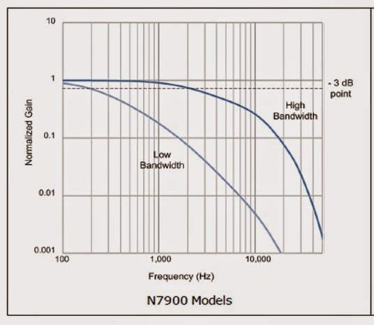
Figure 1: N7900A APS small signal resistive loading output voltage response

Low setting provides maximum stability and so it accommodates a wider range of capacitive loading. High 1 setting in comparison is stable for a smaller range of capacitive loading, but allowing greater response bandwidth. This can be seen in table 1 below, for the recommended capacitive loading for the N7900A APS, again taken from the APS user’s guide.


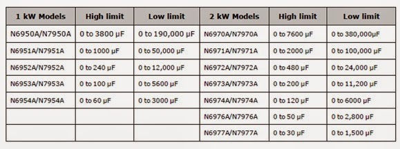
Table 1: N7900A APS recommended maximum capacitive loading

While a maximum capacitive value is shown for each of the different APS models for each of the two settings, this is not altogether as rigid and fixed as it may appear. What is not so obvious is this is based on the load remaining capacitive over a frequency range roughly comparable to the power supply’s response bandwidth or beyond. Because of this the capacitor’s ESR (equivalent series resistance) is an important factor. Beyond the corner frequency determined by the capacitor’s capacitance and ESR, the capacitor looks resistive. If this frequency is considerably lower than the power supply’s response bandwidth, then it has little to no effect on the power supply’s stability. This is the reason why the power supply is able to charge and 
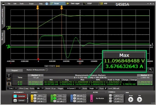
discharge a super capacitor, even though its value is far greater than the capacitance limit given, and not run into stability problems, for example.

One last consideration for more demanding applications needing fast dynamic output changes, either when changing values or generating ARBs is the current needed for charging and discharging capacitive loads.  Capacitors increasingly become “short-circuits” to higher AC frequencies, requiring the power supply to be able to drive or sink very large currents in order to remain effective as a dynamic voltage source!

.

Monday, March 23, 2015

Use slew rate control to cleanly power up and reduce peak inrush current of your DUTs

Previously on Watt’s Up? a colleague wrote about how the current limit setting affects a power supply’s voltage response time (click here to review). In this posting he clearly shows how a low current limit setting can greatly slow down the output voltage turn on response time when powering up your DUT.

While this is generally true and good advice, especially for basic performance power supplies, there are additional things to consider when working with high performance power supplies models, as you will see.

Many basic performance power supplies tend to have larger output filter capacitors in order to achieve lower output noise performance. A disadvantage of having a large output capacitor is that it slows down the output voltage response speed of the power supply. Basic performance power supplies can have turn on response times on the order of a 100 milliseconds.

High performance power supplies operate by a somewhat different set of rules. In comparison to basic performance power supplies they typically have much smaller output capacitors and they are designed to have output turn on and turn off response times on the order of a millisecond or less.

However, absolute fastest is not always the best and that is why fast, high performance power supplies also usually incorporate an output voltage slew rate control as well. This allows you to optimize the output turn on and turn off speed for your particular application. This lets you take advantage of the faster output speed you have available, without it being overkill and cause other problems.

The two most common problems that arise when powering up and powering down many DUTs are related to charging and discharging the input filter capacitor incorporated into them. They are:
  • High peak inrush (and discharge) currents due to the high dV/dt slew rate being applied
  • Power supply CC-CV mode cross over issues resulting from the high peak inrush current


To illustrate, the turn on characteristic of our N6762A power supply was captured when powering up a load consisting of a 1,200 microfarad capacitor in parallel with a 10 ohm resistor. The N6762A was set to 10 volts and its voltage slew rate set to maximum.  This was captured using the N6762A’s digitizing voltage and current readback together with the 14585A software, shown in Figure 1.


Figure 1: N6762A power supply turn on response set to maximum slew rate into parallel RC load

The vertical markers have been placed at zero and maximum voltage points of the turn on ramp. The peak inrush current reaches 3.7 amps and the peak voltage overshoots to 11.06 volts, 10% over the 10 volt setting. The overshoot is a result of the power supply crossing over into current limit during the ramp up and allowing the voltage to rise to 11.06 volts before the voltage control loop regains control to bring the output back down to 10 volts. It also takes a little while for the voltage to settle after the peak overshoot. Both the overshoot voltage and peak inrush current can be problems when powering up a DUT. These occur as a result of having too fast of a voltage slew rate when powering the DUT.

To address the problem we then set the N6762A’s slew rate to a more acceptable value of 2,000 volts/second. The turn on voltage and current were again captured and are shown in Figure 2. As can be seen the voltage overshoot is eliminated and the inrush current has been reduced to a more moderate 3.3 amps.


Figure 2: N6762A power supply turn on response set to 2,000 V/s slew rate into parallel RC load

So in closing high performance power supplies have a significant advantage in their output response speed, in comparison to basic power supplies. And while faster is usually better, absolute fastest may not be best, and this applies to the output response time of power supplies as well! But by having the ability to set the output slew rate on high performance power supplies gives you the ability to optimize its speed for your given application, providing for the best possible outcome possible!

.

Friday, September 6, 2013

How fundamental features of power supplies impact your test throughput – Part 1

When it comes to manufacturing of electronic products, reducing test time to improve throughput is virtually always a top priority, because “time is money” as the old saying goes! Usually most all of the attention may be placed on reducing the test time of the banner aspects of the product, such as the RF performance of a wireless device, for example. However, the choice of the DC system power supply can also have a huge impact on your test time and throughput during manufacturing. You may find the lowest cost, more basic-performance DC power supply that meets your immediate needs end up costing you the difference in price many, many times over of that of a higher-performance DC power supply having better throughput performance in the long run!

The DC power supply can incorporate a number of advanced features, such as elaborate triggering and sequencing systems, which will allow you restructure your testing to optimize throughput. However, even fundamental throughput-related features of the power supply can also have a large impact on your test time, including:
  • Command processing time
  • Output up-programming time
  • Output down-programming time
  • Measurement time

Figure 1 illustrates what the command processing and up-programming times are for a DC power supply. The command processing time is the time from when the command is first received to the point where the power supply starts acting on it. In this case it is when power supply’s output starts to change. The up-programming response time is the time the power supply takes for the output to rise and settle within a small band around the final output level, after processing the command instructing it to change its output level.


Figure 1: Power supply command processing and up-programming response times

The down-programming response time is like the up-programming response time except that the power supply is instead being programmed to a lower level. However, you need to look at down-programming independently as short up-programming time does not necessarily guarantee comparably short down-programming time. More basic performance DC power supplies usually lack an active down-programmer circuit that quickly brings down the output. In this case the down-programming response time can be very dependent on how much load the DUT presents to the power supply’s output.

How much difference is there in performance between more basic performance and higher performance DC power supplies on these throughput-related features? It can be considerable; over several orders of magnitude difference. As one example, command processing time can range from up to 100’s of milliseconds for entry-level power supplies to under 1 millisecond for high performance power supplies.
Another fundamental throughput-related feature of a DC power supply is its measurement time. There are a couple of aspects to consider here as well, which I will elaborate on in part 2 of this series on how fundamental features of power supplies impact your test throughput, in an upcoming posting here on “Watt’s Up?” along with tying it all together to show how they affect actual test throughput!