Showing posts with label transient response. Show all posts

Monday, August 31, 2015

What is meant by a “fast” power supply?

We regularly get requests for a power supply with a “fast” output. This means different things to different people, so we always have to ask clarifying questions. Not only do we need to find out what change needs to happen quickly, but we need to quantify the need and find out how quickly it needs to change. For example, recently, a customer testing power amplifiers wanted to know how quickly a particular power supply could attain its output voltage. Two ways to look at this are:

1. How long does it take for a power supply output voltage to change from one value to another value?
2. How long does it take for a power supply output voltage to recover to its original value following a load current change?

This customer wanted to know the answer to question 1. Luckily, both of these answers can be found in our specifications and supplemental characteristic tables.

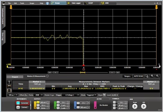
Question 1 is referring to a supplemental characteristic that has a variety of similar names: programming speed, settling time, output response time, output response characteristic, and programming response time. This is typically described with rise time and fall time values, or settling time values, or occasionally with a time constant. Rise (and fall) time values are what you would expect: the time it takes for the output voltage to go from 10% of its final value to 90% of its final value. Settling time (labeled “Output response time” in the graph below) is the time from when the output voltage begins to change until it settles within a specified settling band around the final value, such as 1% or even 0.1%, or sometimes within an LSB (least significant bit) of the final value. My fellow blogger, Ed, posted about how this affects throughput (click here) back in September of 2013.

Question 2 is referring to a specification called transient response, or load transient recovery time. Whenever the load current changes from a low current to a higher current, the output voltage temporarily dips down slightly and then quickly recovers back to the original value (or close to it).
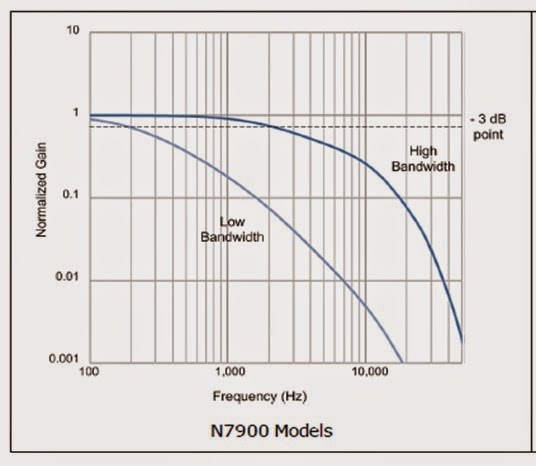
The feedback loop design inside the power supply determines how quickly the voltage recovers from this load current change. Higher bandwidth designs recover more quickly but are less stable. Likewise, lower bandwidth designs recover more slowly and are more stable. Ed posted about optimizing the output response back in April of this year (click here).

So the transient response recovery time is the time from when the load current begins to increase (coincident with the output voltage beginning to drop) to when the output voltage settles within a specified settling band around the final voltage value.

Our customer was interested in a “fast” power supply, meaning one with a settling time to meet his needs. Once we understood what he needed, we directed him to a power supply that could easily meet his requirements!


Tuesday, April 28, 2015

Optimizing a Power Supply’s Output Response Speed for Applications Demanding Higher Performance

Most basic performance power supplies are intended for just providing DC power and maintain a stable output for a wide range of load conditions. They often have lower output bandwidth to achieve this, with the following consequences:
  • Internally this means the feedback loop gain rolls off to zero at a lower frequency, providing relatively greater phase margin. Greater phase margin allows the power supply to remain stable for a wider range of loads, especially larger capacitive loads, when operating as a voltage source.
  • Externally this means the output moves slower; both when programming the output to a new voltage setting as well as when recovering from a step change in output load current.


While this is reasonably suited for fairly static DC powering requirements, greater dynamic output performance is often desirable for a number of more demanding applications, such as:
  • High throughput testing where the power supply’s output needs to change values quickly
  • Fast-slewing pulsed current loads where the transient voltage drop needs to be minimized
  • Applications where the power supply is used to generate power ARB waveforms


A number of things need to be done to a power supply so that it will have faster, higher performance output response speed. Primarily however, this is done by increasing its bandwidth, which means increasing its loop gain and pushing the loop gain crossover out to a higher frequency. The consequence of this the power supply’s stability can be more influenced by the load, especially larger capacitive loads.

To better accommodate a wide range of different loads many of our higher performance power supplies feature a programmable bandwidth or programmable output compensation controls. This allows the output to be set for higher output response speed for a given load, while maintaining stable operation at the same time. As one example our N7900A series Advanced Power System (APS) has a programmable output bandwidth control that can be set to Low, for maximum stability, or set to High1, for much greater output voltage response speed. This can be seen in the graph in Figure 1, taken from the APS user’s guide.


Figure 1: N7900A APS small signal resistive loading output voltage response

Low setting provides maximum stability and so it accommodates a wider range of capacitive loading. High 1 setting in comparison is stable for a smaller range of capacitive loading, but allowing greater response bandwidth. This can be seen in table 1 below, for the recommended capacitive loading for the N7900A APS, again taken from the APS user’s guide.


Table 1: N7900A APS recommended maximum capacitive loading

While a maximum capacitive value is shown for each of the different APS models for each of the two settings, this is not altogether as rigid and fixed as it may appear. What is not so obvious is this is based on the load remaining capacitive over a frequency range roughly comparable to the power supply’s response bandwidth or beyond. Because of this the capacitor’s ESR (equivalent series resistance) is an important factor. Beyond the corner frequency determined by the capacitor’s capacitance and ESR, the capacitor looks resistive. If this frequency is considerably lower than the power supply’s response bandwidth, then it has little to no effect on the power supply’s stability. This is the reason why the power supply is able to charge and discharge a super capacitor, even though its value is far greater than the capacitance limit given, and not run into stability problems, for example.

One last consideration for more demanding applications needing fast dynamic output changes, either when changing values or generating ARBs is the current needed for charging and discharging capacitive loads.  Capacitors increasingly become “short-circuits” to higher AC frequencies, requiring the power supply to be able to drive or sink very large currents in order to remain effective as a dynamic voltage source!

.

Wednesday, August 20, 2014

Some differences between constant current (CC) and constant resistance (CR) loading on your DUT’s performance

Most electronic loads provide constant current (CC), constant resistance (CR) and constant voltage (CV) loading. Some also offer constant power (CP) loading as well. The primary reason for this is this gives the test engineer a choice of loading that best addresses the loading requirement for the DUT, which invariably is some kind of power source.

Most usually the device should be tested with a load that reflects what the loading is like for its end use. In the most common case of a device being predominantly a voltage source the most common loading choices are either CC or CR loading, which we will look at in more detail here. Some feel they can be used interchangeably when testing a voltage source. To some extent this is true but in some cases only one or the other should be used as they can impact the DUT’s performance quite differently.

Let’s first consider static performance. In Figure 1 we have the output characteristics of an ideal voltage source with zero output resistance (a regulated power supply, for example) and a non-ideal voltage source having series output resistance (a battery, for example).  Both have the same open circuit (no load) voltage. Superimposed on these two source output characteristics are two load lines; one for CC and one for CR. As can be seen they are set to draw the same amount of current for the ideal voltage source. However, for the non-ideal voltage source, while the CC load still continues to draw the same amount of current in spite of the voltage drop, not surprisingly the CR load draws less current due to its voltage-dependent nature.


Figure 1: CC and CR loading of ideal and non-ideal voltage sources

CC loading is frequently used for static power supply tests for a key reason. Power supplies are usually specified to have certain output voltage accuracy for a fixed level of current. Using CC loading assures the loading condition is met, regardless of power supply’s output voltage being low or high, or in or out of spec. Non-ideal voltage sources, like batteries, present a little more of a problem and are often specified for both CC and CR loading as a result, to reflect the nature of the loading they may be subjected to in their end use. Due to a battery's load-dependent output voltage, trying to use one type of loading in place the other becomes an iterative process of checking and adjusting loading until the acceptable operating point is established.

Let’s now consider dynamic performance.  CC loading generally has a greater impact on a power supply’s ability to turn on as well as its transient performance and stability, in comparison to CR loading. When the power supply first starts up its output voltage is at zero. A CR load would demand zero current at start up. In comparison a CC load still demands full current. Some power supplies will not start up properly under CC loading. With regard to transient response and stability, CR loading provides a damping action, increasing current demand when the transient voltage increases and decreases demand when the transient voltage decreases, because the current demand is voltage dependent. CC loading does not do this, which can negatively influence transient response and stability somewhat. Whether CC or CR loading is used depends on what the power supply’s specifications call out for the test conditions. Batteries have some dynamic considerations as well. Their output response can be modeled as a series of time constants spanning a wide range of time. This presents somewhat of a moving target for an algorithm that uses an iterative approach to settling on an acceptable operating point.


This is just a couple of examples of how a load’s characteristic affects the performance of the device it is loading, and why electronic loads have multiple operating modes to select from, and worth giving thought next time towards how your device is affected by its loading!

Tuesday, July 22, 2014

What does it mean when my Agilent power supply displays “Osc”?

When using certain higher performance power supplies from Agilent, like the N678xA series source-measure modules, you may discover that the output has shut down and an annunciator displaying “Osc” shows up on the front panel meter display, like that shown in Figure 1 for the N6705B DC Power Analyzer mainframe. 


Figure 1: DC Power Analyzer front panel meter displaying “Osc” on channel 1 output

As you would likely guess, Osc stands for oscillation and this means the output has been shut down for an oscillation fault detection. In this particular instance an N6781A high performance source measure module was installed in channel 1 of the N6705B DC Power Analyzer mainframe.

The N678xA series source measure modules have very high bandwidth so that they can provide faster transient response and output slew rates. However, when the bandwidth of the power supply is increased, its output stability becomes more dependent on the output wiring and DUT impedances. To provide this greater bandwidth and at the same time accommodate a wider range of DUTs on the N678xA modules, there are multiple compensation ranges to select from, based on the DUT’s input capacitance, as shown in the advanced source settings screen in Figure 2.


Figure 2: DC Power Analyzer front panel displaying advanced source settings for the N678xA

Note that “Low” compensation range supports the full range of DUT loading capacitance but this is the default range. While it provides the most robust stability, it does not have the faster response and better performance of the “High” compensation ranges.

As long as the wiring to the DUT is correctly configured and an appropriate compensation range is selected the output should be stable and not trip the oscillation protection system. In the event of conditions leading to an unstable condition, any detection of output oscillations starting up quickly shut down the output in the manner I captured in Figure 3. I did this by creating an instability by removing the load capacitance.


Figure 3: Oscillation protection being tripped as captured in companion 14585A software

In rare circumstances, such as with some DUTs drawing extremely high amplitude, high frequency load currents, which may lead to false tripping, the oscillation protection can be turned off, as shown in Figure 4.


Figure 4: N678xA oscillation protection disable in N6705B DC Power Analyzer advance protection screen

Oscillation protection is a useful mechanism that can protect your DUT and your power supply from an excessively high AC voltage and current due to unstable operating conditions. Now you know what it means next time you see “Osc” displayed on the front panel of you Agilent power supply and what you need to do to rectify it!

.

Monday, December 10, 2012

More on power supply current source-to-sink crossover characteristics


On my earlier posting “Power supply current source-to-sink crossover characteristics” I showed what the effects on the output voltage of a unipolar two-quadrant-power supply were, resulting from the output current on the power supply transitioning between sourcing and sinking. In that example scenario, the power supply was maintaining a constant output voltage and the transitioning between sourcing and sinking current was dictated by the external device connected to and being powered by the power supply. This is perhaps the most common scenario one will encounter that will drive the power supply between sourcing current and sinking current.

Other scenarios do exist that will drive a unipolar two-quadrant power supply to transition between sourcing and sinking output current. One scenario is nearly identical to the earlier posting. However, instead of the device transitioning its voltage between being less and greater than the power supply powering it, the power supply instead transitions its voltage between being less and greater than the active device being normally powered.  A set up for evaluating this scenario on an Agilent N6781A two-quadrant DC source is depicted in Figure 1.


Figure 1: Evaluating current source-to-sink crossover on an N6781A operating in constant voltage

In this scenario having the DC source operating as a voltage source and transitioning between 1.5 and 4.5 volts causes the current to transition between -0.75 and +0.75A.  The voltage and current waveforms captured on an oscilloscope are shown in Figure 2.


Figure 2: Voltage and current waveforms for the set up in Figure 1

The waveforms in Figure 2 are as what should be expected. The actual transition points are where the current waveform passes through zero on the rising and falling edge. An expanded view to the current source-to-sink transition is shown in Figure 3.


Figure 3: Expanded voltage and current waveforms for the set up in Figure 1

As can be seen the voltage ramp transitions smoothly at the threshold point, or zero crossing point, of the current waveform. The reason being is that the DC is maintaining its operation as a voltage source. Its voltage feedback loop is always in control.


Yet one more scenario that will drive a unipolar two-quadrant source to transition between sourcing and sinking current is operate it as a current source and program is current setting between positive and negative values. In this case the device under test that was used is a voltage source.  One real-world example is cycling a rechargeable battery by alternately applying charging and discharging currents to it. The set up for evaluating this scenario, again using an N6781A two-quadrant DC source is depicted in Figure 4.


Figure 4: Evaluating current source-to-sink crossover on an N6781A operating in constant current

For Figure 4 the N6781A was set to operate in constant current and programmed to alternately transition between -0.75A and +0.75A current settings. The resulting voltage and current waveforms are shown in Figure 5.


Figure 5: Voltage and current waveforms for the set up in Figure 4

The waveforms in Figure 5 are as what should be expected. The actual transition points are where the current waveform passes through zero on the rising and falling edge. An expanded view to the current source-to-sink transition is shown in Figure 6.


Figure 6: Expanded voltage and current waveforms for the set up in Figure 4

As the N6781A is operating in current priority the interest is in how well it controls its current while transitioning through the zero-crossing point. As observed in Figure 6 it transitions smoothly through the zero-crossing point. The voltage performance is determined by the DUT, not the N6781A, as the N6781A is operating in constant current.

So what was found here is, for a unipolar two-quadrant DC source, transitioning between sourcing and sinking current should generally be virtually seamless as, under normal circumstances, should remain in either constant voltage or constant current during the entire transition.

Wednesday, December 5, 2012

Power supply current source-to-sink crossover characteristics


A two-quadrant power supply is traditionally one that outputs unipolar voltage but is able to both source as well as sink current. For a positive polarity power source, when sourcing current it is operating in quadrant 1 as a conventional power source. When sinking current it is operating in quadrant 2 as an electronic load. Conversely, a negative polarity two-quadrant  power source operates in quadrants three and four. Further details on power supply operating quadrants are provided in a recent posting here in ‘Watt’s Up?”, What is a bipolar (four-quadrant) power supply? Often a number of questions come up when explaining two-quadrant power supply operation, including:
  • What does it take to get the power supply operating as a voltage source to cross over from sourcing to sinking current?
  • What effect does crossing over from sourcing to sinking current have on the power supply’s output?


For a two-quadrant voltage source to be able to operate in the second quadrant as an electronic load, the device it is normally powering must also be able to source current and power as well as normally draw current and power. Such an arrangement is depicted in Figure 1, where the device is normally a load, represented by a resistance, but also has a charging circuit, represented by a switch and a voltage source with current-limiting series resistance.


Figure 1: Voltage source and example load device arrangement for two-quadrant operation.

There is no particular control on a two-quadrant power supply that one has to change to get it to transition from sourcing current and power to sinking current and power from the device it is normally powering. It is simply when the source voltage is greater than the device’s voltage then the voltage source will be operating in quadrant one sourcing power and when the source voltage is less than the device’s voltage the voltage source will be operating in quadrant two as an electronic load. In figure 1, during charging the load device can source current back out of its input power terminals as long as the charger’s current-limited voltage is greater than the source voltage.

It is assumed that load device’s load and charge currents are lower than the positive and negative current limits of the voltage source so that the voltage source always remains in constant voltage (CV) operation. A step change in current is the most demanding from a transient standpoint, but as the voltage source is always in its constant voltage mode it handle the transition well as its voltage control amplifier is always in control. This is in stark contrast to a mode cross over between voltage and current where different control amplifiers need to exchange control of the power supply’s output. In this later case there can be a large transient while changing modes. See another posting, Why Does My Power Supply Overshoot at Current Limit? Insights on Mode Crossover” for further information on this.  There is a specification given on voltage sources which quantifies the impact one should expect to see from a step change in current going from sourcing current to sinking current, which is its transient voltage response.  A transient voltage response measurement was taken on an N6781A two-quadrant DC source, stepping the load from 0.1 amps to 1.5 amps, roughly 50% of its rated output current.


Figure 2: Agilent N6781A transient voltage response measurement for 0.1A to 1.5A load step

However, the transient voltage response shown in Figure 2 was just for sourcing current. With a well-designed two-quadrant voltage source the transient voltage response should be virtually unchanged for any step change in current load, as long as it falls within the voltage source’s current range.  The transient voltage response for an N6781A was again capture in Figure 3, but now for stepping the load between -0.7A and +0.7A.


Figure 3: Agilent N6781A transient voltage response measurement for -0.7A to +0.7A load step

As can be seen in Figures 2 and 3 the voltage transient response for the N6781A remained unchanged regardless of whether the stepped load current was all positive or swung between positive and negative (sourcing and sinking).

While the transient voltage response addresses the dynamic current loading on the voltage source there is another specification that addresses the static current loading characteristic, which is the DC load regulation or load effect.  This is a very small effect on the order of 0.01% output change for many voltage sources. For example, for the N6781A the load effect in its 6 volt range is 400 microvolts for any load change. In the case of the N6781A being tested here the DC change was the same for both the 0.1 to 1.5 amp step and the -0.7 to +0.7 amp step change.


There are two more scenarios which will cause a two-quadrant power supply transition between current sourcing and sinking.  The first is very similar to above with the two-quadrant power supply operating in constant voltage (CV) mode, but instead of the DUT changing, the power supply changes its voltage level instead.  The final scenario is having the two-quadrant power supply operating in constant current with the DUT being a suitable voltage source that is able to source and sink power as well, like a battery for example. Here the two-quadrant power supply can be programmed to change from a positive current setting to a negative current setting, thus transitioning between sourcing and sinking current again, and its current regulating performance is now a consideration.  Both good topics for future postings!

Tuesday, December 6, 2011

Should I Use a Switching or Linear DC Power Supply For My Next Test System? (part 4 of 4)

Part 4 of 4: Making the Comparison and Choice
In the first three parts of this post we looked at the topologies and merits of linear DC power supplies, traditional and high-performance switching DC power supplies, and common mode noise current considerations of each. So now in this final part we have reached a point where we can hopefully make an informed comparison and choice. Tables 1 and 2 summarize several key qualitative and quantitative aspects of all three DC power supply types, based on what we have learned.
Table 1: Qualitative comparison of DC power supply topologies

Table 2: Quantitative comparison of DC power supply topologies

So what DC power supply topology is the best choice for your next test system? In the past it usually ended up having to be a linear topology to meet performance requirements in most all but very high power, lower performance test situations. However, high-performance switching DC power supplies have nowadays for the most part closed the performance gap with linear DC power supplies. And, at higher power, the favorable choice may come down to selecting between several different switching DC power supplies only, due to their cost, size, and availability. So the answer is you need to make a choice based on how well the power supply meets your performance, space, and cost requirements, rather than basing the choice on its topology. Except for the most demanding low power test applications, like those needing the performance of a source measure unit (SMU), chances are much higher these days that the next DC power supply you select for your next test system you will be a switcher (and you possibly may not even realize it). What has been your experience?

Tuesday, November 29, 2011

Should I Use a Switching or Linear DC Power Supply For My Next Test System? (part 3 of 4)

Part 3 of 4: DC Power Supply Common Mode Noise Current Considerations
Common mode noise current is a fact of life that manifests itself in many ways in test systems. There are several mechanisms that couple unwanted common mode noise currents into ground loops. An excellent overview on this is given in a two part post on the General Purpose Test Equipment (GPETE) blog “Ground Loops and Other Spurious Coupling Mechanisms and How to Prevent Them” (click here). However this is also an important consideration with our choice of a DC system power supply for testing as they are a source of common mode noise current. This is one area where linear DC power supplies still outperform switching DC power supplies. This can become a concern in some highly noise-sensitive test applications. As shown in Figure 1 the common mode noise current ICM is a noise signal that flows out of both output leads and returns through earth. By nature it is considered to be a current signal due to its relatively high associated impedance, ZCM.

Figure 1: Common Mode Noise Current and Path

Common mode noise current is often much greater in traditional switching DC power supplies. High voltage slewing (dv/dt) of the switching transistors capacitively couples through to the output, in extreme cases generating up to hundreds of milliamps pk-pk of high frequency current. In comparison, properly designed linear DC power supplies usually generate only microamps pk-pk of common mode noise current. It is worth noting even a linear DC power supply is still capable of generating several milliamps pk-pk of common mode noise current, if not properly designed. High-performance switching DC power supplies are much closer to the performance of a linear. They are designed to have low common mode noise current, typically just a few milliamps.

Common mode noise current can become a problem when it shows up as high frequency voltage spikes superimposed on the DC output voltage. This depends on the magnitude of current and imbalance in impedances in the path to the DUT. If large enough, this can become more troublesome than the differential mode noise voltage present. Generally, the microamp level of a linear DC power supply is negligible, while hundreds of milliamps from a traditional switching DC power supply may be cause for concern. Because common mode noise current is often misunderstood or overlooked, one may be left with a false impression that all switching DC power supplies are simply unsuitable for test, based on a bad experience with using one, not being aware that its high common mode noise current was actually the underlying cause.

In practice, at typical levels, common mode noise current often turns out not to be an issue. First, many applications are relatively insensitive to this noise. For example, equipment in telecommunications and digital information systems are powered by traditional switching DC power supplies in actual use and are reasonable immune to it. Second, where common mode noise current is more critical, the much lower levels from today’s high-performance switching DC power supplies makes it a non-issue in all but the most noise sensitive applications.

In those cases where common mode noise current proves to be a problem, as with some extremely sensitive analog circuitry, adding filtering can be a good solution. You can then take advantage of the benefits a switching DC power supply has to offer. A high-performance switching DC power supply having reasonably low common mode current can usually be made to work without much effort in extremely noise-sensitive applications, using appropriate filtering, capable of attenuating the high frequency content present in the common mode noise current. Such filtering can also prove effective on other high frequency noises, including AC line EMI and ground loop pickup. These other noises may be present regardless of the power supply topology.

Coming up next is the fourth and final part where we make our overall comparison and come to a conclusion on which power supply topology is best suited for test.

References:
1. Taking The Mystery Out Of Switching-Power-Supply Noise Understanding the source of unspecified noise currents and how to measure them can save your sanity
By Craig Maier, Hewlett Packard Co. © 1991 Penton Publishing, Inc.

Wednesday, November 23, 2011

Should I Use a Switching or Linear DC Power Supply For My Next Test System? (part 2 of 4)

Part 2 of 4: Switching DC system power supply attributes
In part 1 we looked at the topology and merits of a linear DC power supply. To be fair we now have to give equal time to discuss the topology and merits of a switching DC system power supply, to make a more informed choice of what will better suit our needs for powering up and testing our devices.

Traditional switching DC power supply topology
The basic traditional switching power supply depicted in Figure 2 is a bit more complex compared to a linear power supply:
1. The AC line voltage is rectified and then filtered to provide an unregulated high voltage DC rail to power the following DC-to-DC inverter circuit.
2. Power transistors switching at 10’s to 100’s of kHz impose a high voltage, high frequency AC pulse waveform on the transformer primary (input).
3. The AC pulse voltage is scaled by the transformer turns ratio to a value consistent with the required DC output voltage.
4. This transformer secondary (output) AC voltage is rectified into a pulsed DC voltage.
5. An LC (inductor-capacitor) output filter averages the pulsed voltage into a continuous DC voltage at the power supply’s output.
6. As with a linear power supply, an error amplifier compares the DC output voltage against a reference to regulate the output at the desired setting.
7. A modulator circuit converts the error amplifier signal into a high frequency, pulse width modulated waveform to drive the switching power transistors.


Figure 2: Basic switching DC power supply circuit

In spite of being more complex the key thing is its much higher operating frequency, several orders of magnitude over that of a linear power supply, greatly reduces the size of the magnetic and filtering components. As a result traditional switching DC power supplies have some inherent advantages:
• High power conversion efficiency of typically 85%, relatively independent of output voltage setting.
• Small size and lightweight, especially at higher power.
• Cost effective, especially at higher power.

Traditional switching DC power supplies also have some typical disadvantages:
• High output noise and ripple voltage
• High common mode noise current
• Slow transient response to AC line and DC output load changes.


High-performance switching DC power supplies lessen the gap
Traditional switching DC power supply performance is largely a result of optimizing well established switching topologies for cost, efficiency and size, exactly the areas where linear DC power supplies suffer. Performance generally had been a secondary consideration for switching DC power supplies. However, things have now improved to better address the high-performance needs for electronics testing. Incorporating more advanced switching topologies, careful design, and better filtering, high-performance switching DC power supplies compare favorably with linear DC power supplies on most aspects, while still retaining most of the advantages of switchers.

So our choice on whether to use a linear or switching power supply has now gotten a bit more difficult! One area that still differentiates these DC power supply topologies is common mode current noise, worthy of its own discussion, which is exactly what I will do in part 3, coming up next!

Tuesday, November 15, 2011

Should I Use a Switching or Linear DC Power Supply For My Next Test System? (part 1 of 4)

Part 1 of 4: Linear System DC Power Supply Attributes
To kick things off I thought it would be helpful to start with a short series of posts discussing something fundamental we’re often faced with; that is making the choice of whether to use a switching or linear DC power supply to power up our devices under test. In part 1 here I’ll begin my discussion with the topology and merits of linear DC power supplies, as I have heard countless times from others that only a linear power supply will do for their testing, principally due to its low output noise. Of course we do not want to take the chance of having power supply noise affect our devices’ test results. While I agree a linear DC power supply is bound to have very low noise, a well-designed switching DC power supply can have surprisingly good performance. So the choice may not be as simple anymore. The good thing here however is this may give us a lot more to choose from, something that may better meet our overall needs, including size and cost, among other things.

Linear DC Power Supply Topology
A linear DC power supply as depicted in Figure 1 is relatively simple in concept and in basic implementation:
  1. A transformer scales the AC line voltage to a value consistent with the required maximum DC output voltage level.
  2. The AC voltage is then rectified into DC voltage.
  3. Large electrolytic capacitors filter much of the AC ripple voltage superimposed on the unregulated DC voltage.
  4. Series-pass power transistors control the difference between the unregulated DC rail voltage and the regulated DC output voltage. There always needs to be some voltage across the series pass transistors for proper regulation.
  5. An error amplifier compares the output voltage to a reference voltage to regulate the output at the desired setting.
  6. Finally, an output filter capacitor further reduces AC output noise and ripple, and lowers output impedance, for a more ideal voltage source characteristic.

Figure 1: Basic Linear DC Power Supply Topology

Linear DC power supply design is well established with only incremental gains now being made in efficiency and thermal management, for the most part. Its straightforward configuration, properly implemented, has some inherent advantages:

  • Fast output transient response to AC line and output load changes
  • Low output noise and ripple voltage, and primarily having low frequency spectral content
  • Very low common mode noise current
  • Cost competitive at lower output power levels (under about 500 watts)

It also has a few inherent disadvantages:

  • Low power efficiency, typically no better than 60% at full output voltage and decreases with lower output voltage settings
  • Relatively large physical size and weight
  • High cost at higher power (above about 500 watts)

So it sounds like a linear power supply has to be the hands-down winner especially for low power applications. Or not? To make a more-informed choice we need to look at the topology and merits of a switching power supply, which I will be doing in part 2!