Friday, April 27, 2012

Can a standard DC power supply be used as a current source?

The quick answer to this question is, yes, most standard DC power supplies can be used as current sources. However, this question deserves more attention, so what follows is the longer answer.

Most DC power supplies can operate in constant voltage (CV) or constant current (CC) mode. CV mode means the power supply is regulating the output voltage and the output current is determined by the load connected across the output terminals. CC mode means the power supply is regulating the output current and the output voltage is determined by the load connected across the output terminals. When operating in CC mode, the power supply is acting like a current source. So any power supply that can operate in CC mode can be used as a current source (click here for more info about CV/CC operation).

Is a standard power supply a good current source?
An ideal current source would have infinite output impedance (an ideal voltage source would have zero output impedance). No power supply has infinite output impedance (or zero output impedance) regardless of the mode in which it is operating. In fact, most power supply designs are optimized for CV mode since most power supply applications require a constant voltage. The optimization includes putting an output capacitor across the output terminals of the power supply to help lower output voltage noise and also to lower the output impedance with frequency. So the effectiveness of a standard power supply as a current source will depend on your needs with frequency.

At DC, a power supply in CC mode does make a good current source. Typical CC load regulation specifications support this notion (click here for more info about load regulation). For example, an Agilent N6752A power supply (maximum ratings of 50 V, 10 A, 100 W) has a CC load regulation specification of 2 mA. This means that the output current will change by less than 2 mA for any load voltage change. So when operating in CC mode, a 50 V output load change will produce a current change of less than 2 mA. If we take the delta V over worst case delta I, we have 50 V / 2 mA = 25 kΩ. This means that the DC output impedance will always be 25 kΩ or more for this power supply. In fact, the current will likely change much less than 2 mA with a 50 V load change making the DC output impedance in CC mode much greater than 25 kΩ.

Of course, a power supply’s effectiveness as a current source should be judged by the output impedance beyond the DC impedance. See the figure below for a graph of the N6752A CC output impedance with frequency:
If the graph continued in the low frequency direction, the output impedance would continue to rise as a “good” current source should. At higher frequencies, the CC loop gain inside the product begins to fall. As the loop gain moves through unity and beyond, the output capacitor in the supply dominates the behavior of the output impedance, so at high frequencies, the output impedance is lower. So how good the power supply is as a current source depends on your needs with frequency. The higher the output impedance, the better the current source. The output impedance also correlates to the CC transient response (and to a much lesser extent, the output programming response time).

The bottom line here is that in most applications, a standard DC power supply can be used in CC mode as a current source.

Thursday, April 19, 2012

Experiences with Power Supply Common Mode Noise Current Measurements

I wrote an earlier posting “DC Power Supply Common Mode Noise Current Considerations” (click here to review) as common mode noise current can be an issue in electronic test applications we face. This is not so much of an issue with all-linear based power supply designs as it can be for ones incorporating switching based topologies. High performance DC power supplies designed for test applications should have relatively low common mode current by design. I thought this would be a good opportunity to get some more first-hand experience validating common mode noise current. The exercise proved to be a bit of an eye-opener. I tried different approaches and, no surprise; I got back seemingly conflicting results. Murphy was busy working overtime here!

I settled on a high performance, switching-based DC source on having a low common mode noise characteristic of 10 mA p-p and 1 mA RMS over a 20 Hz to 20 MHz measurement bandwidth. To properly make this measurement the general consensus here is a wide band current probe and oscilloscope is the preferred solution for peak to peak noise, and a wide band current probe and wide band RMS voltmeter is the preferred solution for RMS noise. As the wide band RMS voltmeters are pretty scarce here I relied on the oscilloscope for both values for the time being. The advantages of current probes for this testing are they provide isolation and have very low insertion impedance.

I located group’s trusty active current probe and oscilloscope. The low signal level I intended to measure dictated using the most sensitive range providing 10 mA/div (with oscilloscope set to 10 mV/div).
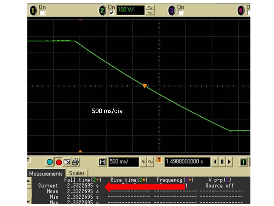
One area of difficulty to anticipate with modern digital oscilloscopes is there are a lot of acquisition settings to contend with, all having a major impact on the actual reading. After sorting all of these out I finally got a base line reading with my DC source turned off, shown in Figure 1.

Figure 1: Common mode noise current base-line reading

My base-line reading presented a bit of a problem. With 1 mV corresponding to 1 mA my 2.5 mA p-p / 0.782 mA RMS base-line values were a bit high in comparison to my expected target values. It would be nicer for this noise floor to be at about 10X smaller so that I don’t have to really factor it out. Resorting to the old trick of looping the wire through the current probe 5 times gave me a 5X larger signal without changing the base-line noise floor. The oscilloscope was now displaying 2 mA /div, with 1 mV corresponding to 0.2 mA. In other words my base-line is now 0.5 mA p-p / 0.156 mA RMS. The penalty for doing this is of course more insertion impedance. Now I was all set to measure the actual common mode noise current. Figure 2 shows the common mode noise current measurement with the DC source on.

Figure 2: Common mode noise current measurement

Things to pay attention to include checking the current on both + and – leads individually to earth ground and load the output with an isolated load (i.e. a power resistor). Full load most often brings on worst case values. Based on the 0.2 conversion ratio I’m now seeing 8 mA p-p and 1.12 mA RMS, including the baseline noise. I am reasonably in the range of the expected values and having a credible measurement!

I decided to compare this approach to making a 50 ohm terminated direct connection. This set up is depicted in Figure 3 below.

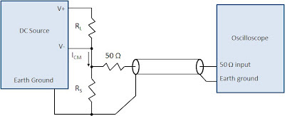
Figure 3: 50 ohm terminated directly connected common mode noise current measurement

I knew insertion impedance was considerably more with this approach so I tried both 10 ohm and 100 ohm shunt values to see what kind of readings I would end up with. Table 1 summarizes the results for the directly connected measurement approach.

Table 1: 50 ohm terminated directly connected common mode noise current results

Clearly the common mode noise current results were nowhere near what I obtained with using a current probe, being much lower, and also highly dependent on the shunt resistor value. Why is that? Looking more closely at the results, the voltage values are relatively constant for both shunt resistor cases. Beyond a certain level of increasing shunt resistance the common mode noise behaves more as a voltage than a current. For this particular DC source the common mode voltage level is extremely low, just a few millivolts.

Not entirely content with the results I was getting I located a different high performance DC source that also incorporated switching topology. No actual specifications or supplemental characteristics had been given for it. When tested it exhibited considerably higher common mode noise than the first DC source. The results are shown in table 2 below.

Table 2: 50 ohm terminated directly connected common mode noise current results, 2nd DC source

With both voltage and current results changing for these two test conditions the common mode noise is exhibiting somewhere between being a noise current versus being a noise voltage. I had hoped to see what the results would be using the current probe but it seemed to have walked away when I needed it!

In Summary:
Making good common mode current noise measurements requires paying a lot of attention to the choice of equipment, equipment settings, test set up, and DUT operating conditions. I still have bit more to investigate but at least I have a much better understanding as to what matters. Maybe in a future posting I can provide what could be deemed as the “golden set up”! To get results that correlate reasonably with any stated values will likely require a set up that exhibits minimal insertion impedance across the entire frequency spectrum. Making directly coupled measurements without the use of a current probe will prove challenging except maybe for DC sources having rather high levels of common mode noise currents

The underlying concern here of course is what is what will be the impact to the DUT due to any common mode noise current from the test system’s DC source. Generally that is any common mode noise current ends up becoming differential mode noise voltage on the DUT’s power input due to impedance imbalances. But one thing I found from my testing is that the common mode noise is not purely a current with relatively unlimited compliance voltage but somewhere between being a noise voltage and noise current, depending on loading conditions. For the first DC source, with what appears to be only a few millivolts behind the current it is unlikely that it would create any issues for even the most sensitive DUTs. For the second DC source however, having 100’s of millivolts behind its current, could potentially lead to unwanted differential voltage noise on the DUT. Further investigation is in order!

Thursday, April 12, 2012

Pay Attention to the Impact of the Bypass Capacitor on Leakage Current Value and Test Time

It is no secret there is big demand for all kinds of wireless battery powered devices and, likewise, the components that go into these devices. These devices and their components need to be very efficient in order to get the most operating and standby time out of the limited amount of power they have available from the battery. Off-mode and leakage currents of these devices and components need to be kept to a minimum as an important part of maximizing battery run and standby time. Levels are typically in the range of tens of microamps for devices and just a microamp or less for a component. Off-mode and leakage currents are routinely tested in production to assure they meet specified requirements. The markets for wireless battery powered devices and their components are intensely competitive. Test times need to be kept to a minimum, especially for the components. It turns out the choice of the input power bypass capacitor being used, either within the DUT on the DUT’s test fixture, can have a large impact on the leakage current value and especially the test time for making an accurate leakage current measurement.

Good things come in small packages?
A lot has been done to provide greater capacitance in smaller packages for ceramic and electrolytic capacitors, for use in bypass applications. It is worth noting that electrolytic and ceramic capacitors exhibit appreciable dielectric absorption, or DA. This is a non-linear behavior causing the capacitor to have a large time-dependent charge or discharge factor, when a voltage or short is applied. It is usually modeled as a number of different value series R-C pairs connected in parallel with the main capacitor. This causes the capacitor to take considerable time to reach its final steady state near-zero current when a voltage is applied or changed. When trying to test the true leakage current on a DUT it may be necessary to wait until the current on any bypass capacitors has reached steady state before a current measurement is taken. Depending on the test time and capacitor being used this could result in an unacceptably long wait time.

So how do they compare?
In Figure 1 I captured the time-dependent current response waveform for a 5.1 megohm resistor, a 5.1 megohm resistor in parallel with 100 microfarad electrolytic capacitor, and finally a 5.1 megohm resistor in parallel with 100 microfarad film capacitor, when a 5 volt step stimulus was applied.

Figure 1: Current response of different R-C loads to 5 volt step

The 5.1 megohm resistor (i.e. “no capacitor”) serves as a base line to compare the affect the two different bypass capacitors have on leakage current measurement. The film capacitor has relatively ideal electrical characteristics in comparison to an equivalent electrolytic or ceramic capacitor. It settles down to near steady state conditions within 0.5 to 1 second. At 3 to 3.5 seconds out (marker placement in Figure 1) the film capacitor is contributing a fairly negligible 42 nanoamps of additional leakage. In comparison the electrolytic capacitor current is still four times as great as the resistor current and nowhere near being settled out. If you ever wondered why audio equipment producers insist on high performance film capacitors in critical applications, DA is one of those reasons!

So how long did it take for the electrolytic capacitor to reach steady state? I set up a longer term capture in Figure 2 for the electrolytic capacitor. After about a whopping 40 seconds later it seemed to be fully settled out, but still contributing a substantial 893 nanoamps of additional steady state leakage current.

Figure 2: 100 microfarad electrolytic capacitor settling time

Where do I go from here?
So what should one do when needing to test leakage current? When testing a wireless device be aware of what kind and value of bypass capacitor has been incorporated into it. Most likely it is a ceramic capacitor nowadays. Film capacitors are too large and cost prohibitive here. Find out how long it takes to settle to its steady state value. Also, off-state current measurements are generally left until the end of the testing to not waste time waiting for the capacitor to reach steady state. If testing a component, if a bypass capacitor is being used on the test fixture, consider using a film capacitor. With test times of just seconds and microamp level leakage currents the wrong bypass capacitor can be a huge problem!

Friday, April 6, 2012

What’s the difference between a fixed output power supply and a programmable output power supply?

I am very fortunate to work with a lot of very smart, talented, and knowledgeable engineers with vast technical backgrounds. I also work with some very smart, talented, and knowledgeable non-technical individuals, some of whom are involved in our sales process. Last month, during a sales training session, one of these individuals identified a competitor’s power supply product that looked very similar to one of our Agilent power supply products: a mainframe with plug-in modules. Upon further investigation, it turned out that the competitor’s product really consisted of modules that were virtually fixed output power supplies while our Agilent product provides programmable output power supplies. So, in fact, these two products do not compete against each other despite the initial appearance. This experience inspired me to post about the differences between a fixed output DC power supply and a programmable output DC power supply.

Fixed output power supplies
A fixed output power supply has, well, a fixed output voltage. This means that when the power supply is plugged in and the output is on, the output voltage is a single voltage that is not expected to change – it is fixed at that voltage. These power supplies are typically used to provide simple bias for a circuit. Some are embedded on a printed circuit board or mounted inside a larger chassis with other circuits, and others may be rack mounted. Fixed output power supplies come in many forms as shown below. Some have a single output voltage while others provide multiple output voltages. One example of a fixed output power supply with multiple outputs is a PC supply (upper left in the figure) – it typically has the following DC output voltages: +3.3 V, +5 V, and +/- 12 V. These voltages provide power to the chips on the PC’s motherboard, including the microprocessor, and to the peripherals installed in the PC, such as the disk drive.

Fixed output power supplies normally have a fixed current limit setting. They typically regulate their output voltages to an accuracy of a few percent (for example, 5%). Many have output noise specifications of 50 to 150 mV peak-to-peak and typically have no measurement capability (such as output voltage or output current measurement).

Programmable output power supplies
A programmable output power supply’s output voltage can be set (programmed) by the user. This means that you can set the voltage to any value between zero and the maximum rated voltage (plus and/or minus) of the supply and change it whenever necessary. The set values are normally controlled either from the front panel of the supply with knobs or buttons, or through the built-in interface connected to a computer. Commands are sent from the computer to the supply to change its output voltage. These power supplies are typically used in test and measurement applications. They might be found on a design engineer’s bench or mounted in a rack of automated test equipment. They come in many forms as shown below. Some have a single output voltage while others provide multiple output voltages. The ability to change the output voltage is required in a circuit test environment. For example, to test a PC’s disk drive, you will need +5 V and + 12 V to power the drive. When installed in a PC, the disk drive will get power from a fixed output power supply in the PC. But when testing the disk drive outside of the PC, you should use a programmable power supply. Since the output voltage of a fixed output supply has an accuracy of a few percent, the voltage could be higher or lower than the nominal. For example, if the +5 V fixed supply has an accuracy of 5%, it could be any value from +4.75 V to +5.25 V. When installed in the PC, the disk drive has to work over this entire range of possible voltages applied to it. So to test it outside of the PC, a programmable power supply should be used and set to various voltages in this range to ensure the drive will always work.


Programmable output power supplies normally have a programmable current limit setting to help protect the device under test from exposure to excessive current. They typically regulate their output voltages to an accuracy of a few tenths of a percent or even better (for example, 0.06%). They have output noise specifications of 1 to 50 mV peak-to-peak and typically have built-in output voltage and output current measurement capability.

Summary
So the main differences between fixed output power supplies and programmable output power supplies are the ability to change the output voltage and the specifications. You can change the output voltage of a programmable supply while that of a fixed supply cannot be changed. Programmable supplies have much more accurate output voltages and much lower noise. They also can typically measure their own output voltage and current while a fixed output supply cannot. Of course, the extra capabilities of the programmable supplies add to their price, but you get what you pay for!

Thursday, March 29, 2012

Protect your DUT with power supply features including a watchdog timer

The two biggest threats of damage to your device under test (DUT) from a power supply perspective are excessive voltage and excessive current. There are various protection features built into quality power supplies that will protect your DUT from exposure to these destructive forces. There are also some other not-so-common features that can prove to be invaluable in certain applications.

Soft limits
The first line of defense against too much voltage or current can be using soft limits (when available). These are maximum values for voltage and current you can set that later prevent someone from setting output voltage or current values that exceed your soft limit settings. If someone attempts to set a higher value (either from the front panel or over the programming interface), the power supply will ignore the request and generate an error. While this feature is useful to prevent accidentally setting voltages or currents that are too high, it cannot protect the DUT if the voltage or current actually exceeds a value due to another reason. Over-voltage protection and over-current protection must be used for these cases.

Over-voltage protection
Over-voltage protection (OVP) is a feature that uses an OVP setting (separate from the output voltage setting). If the actual output voltage reaches or exceeds the OVP setting, the power supply shuts down its output, protecting the DUT from excessive voltage. The figure below shows a power supply output voltage heading toward 20 V with an OVP setting of 15 V. The output shuts down when the voltage reaches 15 V.

Some power supplies have an SCR (silicon-controlled rectifier) across their output that gets turned on when the OVP trips essentially shorting the output as quickly as possible. Again, the idea here is to protect the DUT from excessive voltage by limiting the voltage magnitude and exposure time as much as possible. The SCR circuit is sometimes called a “crowbar” circuit since it acts like taking a large piece of metal, such as a crowbar, and placing it across the power supply output terminals.

Over-current protection
Over-current protection (OCP) is a feature that uses the constant current (CC) setting. If the actual output current reaches or exceeds the constant current setting causing the power supply to go into CC mode, the power supply shuts down its output, protecting the DUT from excessive current. The figure below shows a power supply output current heading toward 3 A with a CC setting of 1 A and OCP turned on. The power supply takes just a few hundred microseconds to register the over-current condition and then shut down the output. The CC and OCP circuits are not perfect, so you can see the current exceed the CC setting of 1 A, but it does so for only a brief time.

The OCP feature can be turned on or off and works in conjunction with the CC setting. The CC setting prevents the output current from exceeding the setting, but it does not shut down the output if the CC value is reached. If OCP is turned off and CC occurs, the power supply will continue producing current at the CC value basically forever. This could damage some DUTs as the undesired current flows continuously through the DUT. If OCP is turned on and CC occurs, the power supply will shut down its output, eliminating the current flowing to the DUT.

Note that there are times when briefly entering CC mode is expected and an OCP shutdown would be a problem. For example, if the load on the power supply has a large input capacitor, and the output voltage is set to go from zero to the programmed value, the cap will draw a large inrush current that could temporarily cause the power supply to go into CC mode while charging the cap. This short time in CC mode may be expected and considered acceptable, so there is another feature associated with the OCP setting that is a delay time. Upon a programmed voltage change (such as from zero to the programmed value as mentioned above), the OCP circuit will temporarily ignore the CC status just for the delay time, therefore avoiding nuisance OCP tripping.

Remote inhibit
Remote inhibit (or remote shutdown) is a feature that allows an external signal, such as a switch opening or closing, to shutdown the output of the power supply. This can be used for protection in a variety of ways. For example, you might wire this input to an emergency shutdown switch in your test system that an operator would use if a dangerous condition was observed such as smoke coming from your DUT. Or, the remote inhibit could be used to protect the test system operator by being connected to a micro switch on a safety cover for the DUT. If dangerous voltages are present on the DUT when operating, the micro switch could disable DUT power when the cover is open.

Watchdog timer
The watchdog timer is a unique feature on some Agilent power supplies, such as the N6700 series. This feature looks for any interface bus activity (LAN, GPIB, or USB) and if no bus activity is detected by the power supply for a time that you set, the power supply output shuts down. This feature was inspired by one of our customers testing new chip designs. The engineer was running long-term reliability testing including heating and cooling of the chips. These tests would run for weeks or even months. A computer program was used to control the N6700 power supplies that were responsible for heating and cooling the chips. If the program hung up, it was possible to burn up the chips. So the engineer expressed an interest in having the power supply shut down its own outputs if no commands were received by the power supply for a length of time indicating that the program has stopped working properly. The watchdog timer allows you to set delay times from 1 to 3600 seconds.

Other protection features that protect the power supply itself
There are some protection features that indirectly protect your DUT by protecting the power supply itself, such as over-temperature (OT) protection. If the power supply detects an internal temperature that exceeds a predetermined limit, it will shut down its output. The temperature may rise due to an unusually high ambient temperature, or perhaps due to a blocked or incapacitated cooling fan. Shutting down the output in response to high temperature will prevent other power supply components from failing that could lead to a more catastrophic condition.

One other way in which a power supply protects itself is with an internal reverse protection diode across its output terminals. As part of the internal design, there is often a polarized electrolytic capacitor across the output terminals of a power supply. If a reverse voltage from an external power source was applied across the output terminals, the cap (or other internal circuitry) could easily be damaged. The design includes a diode across the output terminals with its cathode connected to the positive terminal and its anode connected to the negative terminal. The diode will conduct if a reverse voltage from an external source is applied across the output terminals, thereby preventing the reverse voltage from rising above a diode drop and damaging other internal components.

Wednesday, March 28, 2012

What Is Going On When My Power Supply Displays “UNR”?

Most everyone is familiar with the very traditional Constant Voltage (CV) and Constant Current (CC) operating modes incorporated in most any lab bench or system power supply. All but the most very basic power supplies provide display indicators or annunciators to indicate whether it is in CV or CC mode. However, moderately more sophisticated power supplies provide additional indicators or annunciators to provide increased insight and more information about their operating status. One annunciator you may encounter is seeing “UNR” flash on, either momentarily or continuously. It’s fairly obvious that this means that the power supply is unregulated; it is failing to maintain a Constant Voltage or Constant Current. But what is really going on when the power supply displays UNR and what things might cause this?
To gain better insight about CV, CC and UNR operating modes it is helpful to visualize what is going on with an IV graph of the power supply output in combination with the load line of the external device being powered. I wrote a two part post about voltage and current levels and limits which you may find useful to review. If you like you can access it from these links levels and limits part 1 and levels and limits part 2. This posting builds nicely on these earlier postings. A conventional single quadrant power supply IV graph with resistive load line is depicted in Figure 1. As the load resistance varies from infinity to zero the power supply’s output goes through the full range of CV mode through CC mode operation. With a passive load like a resistor you are unlikely to encounter UNREG mode, unless perhaps something goes wrong in the power supply itself.
Figure 1: Single quadrant power supply IV characteristic with a resistive load

However, with active load devices you have a pretty high chance of encountering UNR mode operation, depending where the actual voltage and current values end up at in comparison to the power supply’s voltage and current settings. One common application where UNR can be easily encountered is charging a battery (our external active load device) with a power supply. Two different scenarios are depicted in Figure 2. For scenario 1, when the battery voltage is less than the power supply’s output, the point where the power supply’s IV characteristic curve and the battery’s load line (a CV characteristic) intersect, the power supply is in CC mode, happily supplying a regulated charge current into the battery. However, for scenario 2 the battery’s voltage is greater than the power supply’s CV setting (for example, you have your automobile battery charger set to 6 volts when you connect it to a 12 volt battery). Providing the power supply is not able to sink current the battery forces the power supply’s output voltage up along the graph’s voltage axis to the battery’s voltage level. Operating along this whole range of voltage greater than the power supply’s output voltage setting puts the power supply into its UNR mode of operation.
Figure 2: Single quadrant power supply IV characteristic with a battery load

A danger here is more sophisticated power supplies usually incorporate Over Voltage Protection (OVP). One kind of OVP is a crowbar which is an SCR designed to short the output to quickly bring down the output voltage to protect the (possibly expensive) device being powered. When connected to a battery if an OVP crowbar is tripped, damage to the power supply or battery could occur due to batteries being able to deliver a fairly unlimited level of current. It is worth knowing what kind of OVP there is in a power supply before attempting to charge a battery with it. Better yet is to use a power supply or charger specifically designed to properly monitor and charge a given type of battery. The designers take these things into consideration so you don’t have to!
I have digressed here a little on yet another mode, OVP, but it’s all worth knowing when working with power supplies! Can you think of other scenarios that might drive a power supply into UNR? (Hint: How about the other end of the power supply IV characteristic, where it meets the horizontal current axis?)

Tuesday, March 27, 2012

If you need fast rise and fall times for your DUT power, use a power supply with a downprogrammer

If you have to provide DC power to a device under test (DUT) and you want the voltage fall time to be just as fast as the rise time, use a power supply with a downprogrammer. A downprogrammer is a circuit built into the output of a power supply that actively pulls the output voltage down when the power supply is moving from a higher setting to a lower setting. Power supplies are good at forcing their output voltage up since that is what their internal circuitry is designed to do. This design results in fast rise times. However, when the supply’s output is changed to move down in voltage, the power supply’s output capacitor (and any additional external DUT capacitance) will need to be discharged. Without a downprogrammer, if there is a light load or no load on the output of the power supply, there is nowhere for the current from the output cap to flow to discharge it. This scenario causes the voltage to take a long time to come down resulting in slow fall times. And this behavior leads to longer test times since you will have to wait for the output voltage to settle to the lower value before you can proceed with your test.

The figures below show an example of the output voltage rise and fall times of a power supply without a downprogrammer under light load conditions. You can see the short rise time (tens of milliseconds) and longer fall time (several seconds).


One of my colleagues, Bob Zollo, wrote an article on this topic that appeared in Electronic Design on February 7, 2012. Here is a link to the article:

http://electronicdesign.com/article/test-and-measurement/If-Your-Power-Supply-Needs-Fast-Rise-And-Fall-Times-Try-A-Down-Programmer-64725

A power supply without an active downprogrammer can have fall times that are tens to hundreds of times longer than a power supply with a downprogrammer. If your test requires you to have fast fall times for your DUT power, or your test requires you to frequently change the voltage on your DUT (both up and down) and throughput is an issue for you, make sure the power supply you choose has a downprogrammer – you won’t have to wait as long for the voltage to move from a higher value to a lower value.