Sunday, March 31, 2013

Remote sensing can affect load regulation performance


Back in September of 2011, I posted about what load effect was (also known as load regulation) and how it affected testing (see http://powersupplyblog.tm.agilent.com/2011/09/what-is-load-effect-and-how-does-it.html). The voltage load effect specification tells you the maximum amount you can expect the output voltage to change when you change the load current. In addition to the voltage load effect specification, some power supplies have an additional statement in the remote sensing capabilities section about changes to the voltage load effect spec when using remote sensing. These changes are sometimes referred to as load regulation degradation.

For example, the Agilent 6642A power supply (20 V, 10 A, 200 W) has a voltage load regulation specification of 2 mV. This means that for any load current change between 0 A and 10 A, the output voltage will change by no more than 2 mV. The 6642A also has a remote sensing capability spec (really, a “supplemental characteristic”). It says that each load lead is allowed to drop up to half the rated output voltage. The rated output voltage for the 6642A is 20 V, so half is 10 V meaning when remote sensing, you can drop up to 10 V on each load lead. Also included in the 6642A remote sensing capability spec is a statement about load regulation. It says that for each 1 volt change in the + output lead, you must add 3 mV to the load regulation spec. For example, if you were remote sensing and you had 0.1 ohms of resistance in your + output load lead (this could be due to the total resistance of the wire, connectors, and any relays you may have in series with the + output terminal) and you were running 10 A through the 0.1 ohms, you would have a voltage drop of 10 A x 0.1 ohms = 1 V on the + output lead. This would add 3 mV to the load regulation spec of 2 mV for a total of 5 mV.

There are other ways in which this effect can be shown in specifications. For example, when remote sensing, the Agilent 667xA Series of power supplies expresses the load regulation degradation as a formula that includes the voltage drop in the load leads, the resistance in the sense leads, and the voltage rating of the power supply. Output voltage regulation is affected by these parameters because the sense leads are part of the power supply’s feedback circuit, and these formulas describe that effect:


One more example of a way in which this effect can be shown in specifications is illustrated by the Agilent N6752A. Its load effect specification is 2 mV and goes on to say “Applies for any output load change, with a maximum load-lead drop of 1 V/lead”. So the effect of load-lead drop is already included in the load effect spec. Then, the remote sense capability section simply says that the outputs can maintain specifications with up to a 1 V drop per load lead.

When you are choosing a power supply, if you want the output voltage to be very well regulated at your load, be sure to consider all of the specifications that will affect the voltage. Be aware that as your load current  changes, the voltage can change as described by the load effect spec. Additionally, if you use remote sensing, the load effect could be more pronounced as described in the remote sensing capability section (or elsewhere). Be sure to choose a power supply that is fully specified so you are not surprised by these effects when they occur.

Watt's Up with Datalogging and Digitizing?


All of our power supplies offer the ability to take an average measurement using either the front panel or the MEAS SCPI commands.  Some of our newer power supplies have some more advanced measurement capabilities.   The two capabilities that we are going to look at today are digitized measurements and datalogging.   Let’s take a short look at each one and then talk about when to use each one.

The digitizer has been in our products for a while now.  With the digitizer, you define three parameters and the measurement uses these parameters to return an array of measurements back to you.  The three parameters are: the number of points, the time interval, and the points offset.  The number of points is pretty simple.  It is the number of measurements that you want to take as well as the size of the array that you are going to read back.  The time interval is the pace of the measurements.  This is also the time between the points in the array.  The points offset is a way that you vary the starting point of the array.  This offset can be negative to return measured points before the trigger or positive to delay the start of the measurement.  The most points that we can measure and the fastest time interval is with our N678xA SMU modules.  These modules have a time interval of 5.12 us and a total number of points of 512 Kpoints (keep in mind that 1 Kpoint is 1,024 points).  This yields a total time of 5.12 us x 512 x 1,024 which yields a result of 2.68 seconds.  So the longest measurement that you can make is 2.68 seconds.  The largest time interval that we can measure is 40,000 seconds.  Setting this with the highest number of points would yield 40,000 s x 512 x 1,024 yields a total acquisition of 20,971,520,000 seconds.  That is 666.83 years! 

The other advanced measurement capability that we are going to talk about is our datalogger.  With the datalogger, you set a total acquisition time and an integration time.  The integration time is the amount of time that the power supply will average measurements.  The measurement system is still running at its maximum digitizing rate but it is averaging those measurements and returning that averaged measurement.  The digitizer on the N6705B DC Power Analyzer also will return the maximum measured value and the minimum measured value of each integration period.  The quickest integration time on the N6705B is 20.48 us.  The only limitation in the amount of data that you can log with the internal datalogger is the file size (the maximum file size is somewhere near 2 gB).  If you want to datalog huge files, you can use the external datalog feature (I wrote another blog post about this) or use our 14585A software where the only limitation is the free space on your hard drive.  The catch on the external datalogger is that that the quickest integration time is 102 us.

So when do you use one over the other?  It is pretty simple.  When you want to make a long term measurement (days, weeks, etc.) at a fast rate you should use the datalogger.  You would use this when you are looking to measure something like long term battery drain.  If you are looking for a more short term, faster measurement you would use the digitizer.  You would use the digitizer to measure something like inrush current. 

These are a few of the great features available in our power supplies.  Please let us know if you have any questions on these features or any of the features of our power supplies.          

Wednesday, March 20, 2013

Open sense lead detection, additional protection for remote voltage sensing


A higher level of voltage accuracy is usually always needed for powering electronic devices under test (DUTs). Many devices provide guaranteed specifications for operating at minimum, nominal, and maximum voltages, so the voltage needs to accurate as to not require unacceptable amounts of guard banding of the voltage settings.

One very significant factor that affects the accuracy of the voltage at the DUT is the voltage drop in the wiring between the output terminals of the power supply and the actual DUT fixture, due to wiring’s inherent resistance, as shown in Figure 1.


 A standard feature of most all system DC power supplies is remote voltage sensing. Instead of the voltage being regulated at the output terminals of the DC power supply’s output terminal, it is instead sensed and regulated at the DUT itself, compensating for the voltage drop in the wiring. Additional details of this are documented in an earlier posting: “Use remote sense to regulate voltage at your load”

While remote voltage sensing addresses the problem of voltage drop in wiring affecting the voltage accuracy at the DUT, it then raises the concern of what happens if one of the sense lines becomes disconnected. Will the DC power supply voltage climb up to it maximum potential causing my DUT to be damaged?  Although this is a very legitimate concern, often the voltage is usually kept within a reasonable range of the setting by a feature referred to as “open sense lead protection”. A deeper dive on the issue of open sense lines and open sense lead protection are discussed at our posting: “What happens if remote sense leads open?”

Even with open sense lead protection and the voltage being kept within a reasonable range of the setting, this can be a concern for some customers who are relying on a high level of DC voltage accuracy at the DUT for test and calibration purposes. One categorical example of this is battery powered devices, where ADC circuits that need to precisely monitor the battery input voltage have to be accurately calibrated. If the voltage from the DC power supply has significant error, the DUT will be miss-calibrated.

One issue with open sense lead protection is it is a passive protection mechanism. It is simply a back up that takes over when a sense line is open. There is no way of knowing the sense lead is open. No error flag is set or fault condition tripped. The voltage being read back is the same as that is being regulated by the voltage sensing error amplifier, which is the same as the set voltage, so all looks fine from a read-back perspective. This is where open sense lead detection takes over. Open sense lead detection is a system that actively checks to see if the sense lines are doing their job. If not it lets the test system know there is a fault.

Open sense detection is not a common feature for most system DC power supplies. As one example we do employ it in our 663xx series Mobile Communications DC Sources as these are used for powering, testing and calibrating battery powered wireless devices. In the case of an open sense line condition it generates a fault condition and it keeps the output of the DC source powered down. It also provides status information on which of the sense lines are open as well.

Tuesday, March 12, 2013

What is a power supply’s over current protect (OCP) and how does it work?


One feature we include in our Agilent system DC power supplies for providing additional safeguard for overload-sensitive DUTs is over current protect, or OCP. While some may think this is something separate and independent of current limiting, OCP actually works in concert with current limiting.

Current limiting protects overload-sensitive DUTs by limiting the maximum current that can be drawn by the DUT to a safe level. There are actually a variety of current limit schemes, depending on the level of protection required to safeguard the DUT during overload. Often the current limit is relatively constant, but sometimes it is not, depending on what is best suited for the particular DUT. Additional insights on current limits are provided in an earlier posting, entitled “Types of current limits for over-current protection on DC power supplies“.

By limiting the current to a set level may DUTs are adequately protect from too much current and potential damage. When in current limit, if the overload goes away the power supply automatically goes back to constant voltage (CV) operation. However, current limit may not be quite enough for some DUTs that are very sensitive to overloads. This is where OCP works together with the current limit to provide an additional level of protection. With OCP turned on, when the DC power supply enters into current limit OCP takes over after a specified time delay and shuts down the output of the DC power supply. The delay time is programmable. This prevents OCP from shutting down the DC power supply from short current spikes and other acceptably short overloads that are not considered harmful. Like over voltage protect or OVP, after tripping the output needs to be disabled and an Output Protect Clear needs to be exercised in order to reset the power supply so that its output can be re-enabled.  Unlike OVP, OCP can be turned on and off and its default is usually off. In comparison, OVP is usually always enabled and cannot be turned off. A typical OCP event is illustrated in Figure 1.


Figure 1: OCP operation

When powering DUTs, either on the bench or in a production test system, it is always imperative that adequate safeguards are taken to protect both the DUT as well as the test equipment from inadvertent damage. Over current protect or OCP is yet another of many features incorporated in system DC power supplies you can take advantage of to protect overload-sensitive DUTs from damage during test!

Thursday, February 28, 2013

Overvoltage protection: some background and history

In my previous post, I talked about some of the differences between sensing an overvoltage condition on the output terminals of a power supply and sensing on the sense terminals. In this post, I want to cover some background and history about overvoltage protection (OVP).

OVP is a feature on a power supply that is used to prevent excessive voltage from being applied to sensitive devices that are being powered by the power supply. If the voltage at the output terminals exceeds the OVP setting, the output of the power supply shuts down, thereby protecting the device from excessive voltage. OVP is always active; you cannot turn it off. If you do not want it to activate, you should set it to a value that is much higher than the maximum voltage you expect at the output of your power supply.

An overvoltage condition can occur due to a variety of reasons:
·         Operator error - an operator can mistakenly set a voltage higher than desired
·         Internal circuit failure – an electronic circuit inside the power supply can fail causing the output voltage to rise to an undesired value
·         External power source – an external source of power, such as another power supply or battery in parallel with the output, could produce voltage that is higher than desired

Some power supply OVP designs include a silicon-controlled rectifier (SCR) across the output that would be quickly turned on if an overvoltage condition was detected. The SCR essentially puts a short circuit across the output to prevent the output voltage from going to a high value and staying there. The SCR circuit is sometimes called a “crowbar” circuit since it acts like taking a large piece of metal, such as a crowbar, and placing it across the power supply output terminals to protect the device under test (DUT) from excessive voltage.

Turning on an SCR across the output of a power supply as a response to an overvoltage condition originated as a result of older linear power supply designs. Linear regulators use a series pass transistor (click here for a post about linear regulators). If the series pass transistor fails shorted, all of the unregulated rail voltage inside the power supply appears across the output terminals. This voltage is higher than the maximum rated voltage of the power supply and can easily damage a DUT. When the OVP is activated, a signal is sent to turn off the series pass transistor. However, if that transistor failed shorted, the turn-off signal will be of no use. In this situation, the only way to protect the DUT is to trigger an SCR across the output to essentially short the output. Of course, the SCR circuit is designed to have a large enough capacity to handle the rail voltage and then the current that will flow when it is tripped. If a series pass transistor fails shorted, the AC input line fuse will sometimes blow when the SCR shorts which will completely disable the power supply protecting the DUT.

More recent power supply designs use switching regulation technology (click here for a post on switching regulators). Switching regulators have multiple power transistors that can fail. However, unlike the linear regulator design, when a switching transistor fails, it does not create a path between the rail voltage and the output terminals. So it is unlikely that a failed switching transistor will cause an OVP. And when an OVP activates for another reason in a switching regulator, all of the switching transistors are told to turn off, preventing any power from flowing to the output. As a result, there is no need for an SCR across the output for added protection against an overvoltage.

Decades ago, when OVP first started to be used on our power supplies (we were Hewlett-Packard back then), the OVP setting was fixed. It was internally set to maybe 10% or 20% above the maximum rated output of the power supply. Later, we provided the power supply user with the ability to crudely control the setting of the OVP by turning a potentiometer accessible through a hole in the front panel (see pictures below). The OVP range was typically adjustable from about 20% to 120% of the maximum rated output voltage of the power supply. When this feature first became available, it was offered as an add-on option for some power supply models. Later still, the front panel manually-adjustable OVP became standard on most high-performance power supplies. With advances in electronics, the OVP adjustability was moved deeper inside the supply and controlled with a DAC through front panel button presses or over an interface such as GPIB. Today, OVP is included in nearly every power supply, is set electronically, and is often a calibrated parameter to improve overall accuracy.

Protect your DUT: use sense leads for overvoltage protection (OVP)


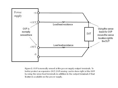
Earlier this week, one of our military customers providing DC power to a very expensive device during test asked about the availability of a special option on one of our power supplies. He wanted the option that changed the location of the overvoltage protection (OVP) sensing terminals from the output terminals of the power supply to the sense terminals of the power supply. Since his device under test (DUT) is located quite a distance away from the power supply, he is using remote sensing to regulate the power supply voltage right at his device under test. (Click here for a post about remote sense.) And since the DUT is very expensive and sensitive to excessive voltage, he needs to protect the input of the DUT from excessive voltage as measured right at the DUT input terminals.

The power supply he is using, an Agilent N6752A installed in an N6700B mainframe, normally uses the output terminals as the sensing location for the overvoltage protection. (Click here for a post that includes a description of OVP.) OVP is used to prevent excessive voltage from being applied to sensitive devices. If the voltage at the output terminals exceeds the OVP setting, the output of the power supply shuts down. Since this customer is very interested in preventing excessive voltage from being applied to his expensive DUT, sensing for an overvoltage condition right at the DUT is important. For the N6752A, Agilent offers a special option (J01) that adds the ability to do OVP sensing with the sense leads. See Figure 1. With the J01 option added to his N6752A, the customer’s DUT is protected against excessive voltage.

You may be wondering why the standard OVP would sense at the output terminals instead of at the sense terminals. For decades, we have been making power supplies that sense OVP at the output terminals. Probably the biggest reason for sensing at the output terminals is because that approach provides more reliable protection than sensing at the sense leads even though it is less accurate. The output terminals are the power-producing terminals. If the sense leads become inadvertently shorted, the voltage at the output terminals would rise uncontrolled beyond the maximum rated output of the power supply. This uncontrolled high voltage could easily damage any device connected to the power supply’s output leads! So sensing for an overvoltage condition at the output terminals actually makes sense. It may not be the most accurate way to protect the DUT, but it is the most reliable given all of the things that can go wrong, such as a wiring error or an internal fault in the power supply.

The J01 option is available for only certain N67xx power modules. It adds the ability to sense for an overvoltage condition on the sense leads. This option does not remove the existing output terminal overvoltage sensing feature; it is in addition to it. Additionally, the J01 option is a tracking OVP option. You set a voltage value that is an offset from the programmed output voltage value. The J01 tracking overvoltage threshold tracks the real-time programming changes to the voltage setting and uses the remote sense leads to monitor the voltage.

Friday, February 15, 2013

Addressing the challenge of sequencing multiple bias supplies on and off


A challenge test engineers are perennially faced with is how to best sequence the bias voltages powering their DUT, when their DUT requires several bias voltages. Many DUTs are sensitive to sequencing and an improper sequence may lead to the DUT hanging up, or worse, suffer damage as a consequence. Not only is sequencing an issue when powering the DUT on, but it can also be an issue when powering the DUT down as well. In addition to sequencing, the slew rates of the various bias voltages can likewise be important to the DUT correctly powering on.

Simply relying on the timing of output-on and output-off commands sent from the test system controller to all the system DC power supplies individually tends to be far too imprecise, especially for critical sequencing timing requirements. The actual turn-on time of a typical system DC power supply can be many tens of milliseconds, and will vary considerably between different models of power supplies. The turn-on and turn-off times of each will need to be carefully characterized in order to know when a command for a specific bias voltage needs to be sent in relation to the other bias voltages. It is very likely the sequence of commands sent for outputs to turn on or off may be in a different sequence to the outputs actually changing, due to delay differences between different DC power supplies! An even bigger problem however is most system controllers are PCs which may randomly experience a large delay in sending out a command, if a higher level service request interrupts and pre-empts execution of the test program.

An alternative approach often taken is adding some custom hardware to control output sequencing. This can assure correct sequencing, but adds a lot of complexity, is usually inflexible, and may introduce other issues and compromises.

At Agilent we added system features to our N6700 series multiple output modular DC power system that support correct power-on and power-off sequencing. The output-on and output-off controls for the individual outputs get grouped together. The N6700 platform knows and compensates for the actual delays of all the various DC power output modules so that the desired delay value entered will be what is accurately achieved. Figure 1 shows setting up an N6705A to achieve a desired turn-on sequence of DC outputs for powering up a PC mother board. Figure 2 shows the actual result. A more detailed description of this PC motherboard example is given in our application note: “Biasing Multiple Input Voltage Devices in R&D”. While the N6705B DC Power Analyzer mainframe is regarded as being primarily for R&D, which this app note is referencing, the low profile rack-mountable N6700 series mainframes have these very same features and suit automated test systems in manufacturing and other environments.


Figure 1: Setting Output Delays


Figure 2: Output Turn-on Sequence Results


Just like setting up the power-on sequence, separate delays for power-off can also be entered, as seen in the set up screen shown in Figure 1, for the expected shut down of the DUT. However, what if there is an emergency shut down due to an abnormal condition and you still want to assure a certain power-off sequence? A colleague worked out the procedure for setting up the N6700 series DC power system to provide an orderly shutdown of the outputs, in the event of a problem on one of the outputs. In this example it happens to be an overvoltage condition on one of the outputs, but any of a number of fault conditions can be acted on to initiate an orderly shutdown. Details of this procedure are provided in another application note; “Avoid DUT Damage by Sequencing Multiple Power Inputs Off Upon a Fault Event”.

So when faced with the challenge of having to properly sequence multiple DC bias voltages powering your DUT, reconsider trying to engineer a solution to accomplish this. Instead, look for features that provide this kind of capability in the system DC power supplies you are looking to use, already built-in. It makes a lot of sense having sequencing built into the power supplies and it will make your life a lot easier!