Thursday, August 28, 2014

What can cause a power supply output voltage to exceed its setting?

We have done a number of posts on power supply protection topics covering both voltage and current issues:

Safeguarding your power-sensitive DUTs from an over power condition

How does power supply overvoltage protection work? 

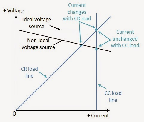
Protect your DUT from over-current in more ways than one

What is a power supply’s over current protect (OCP) and how does it work?

Overvoltage protection: some background and history

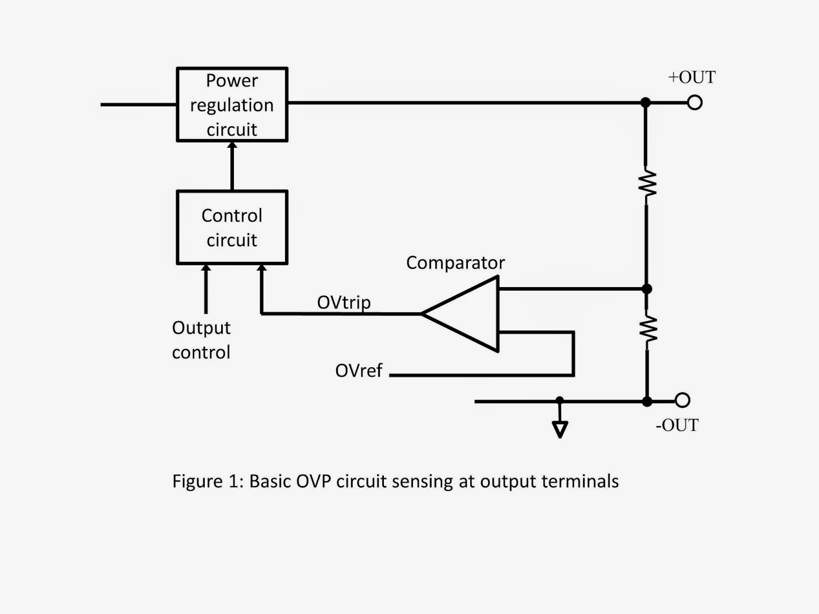
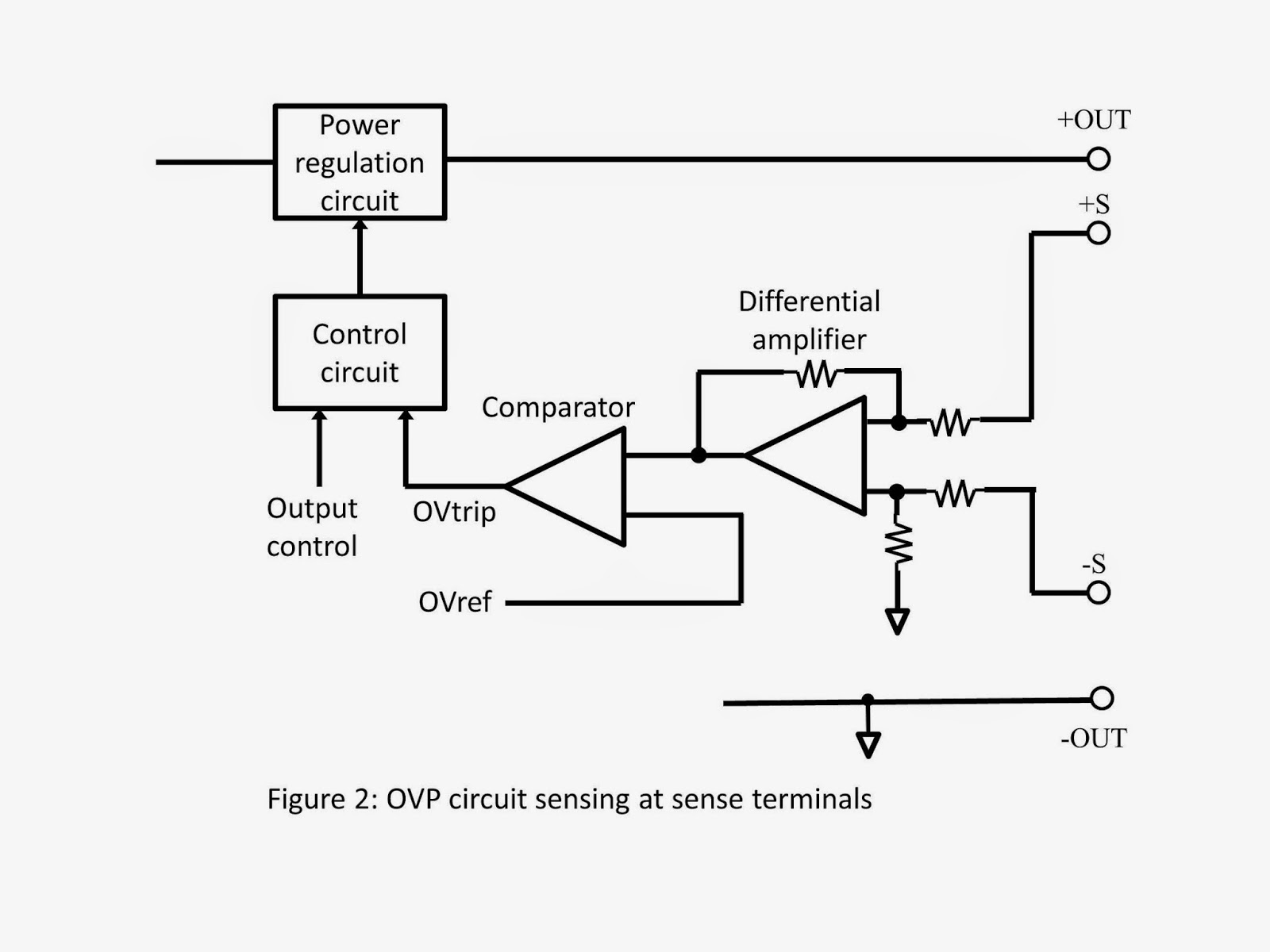
Protect your DUT: use sense leads for overvoltage protection (OVP)

Types of current limits for over-current protection on DC power supplies

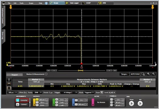
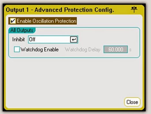
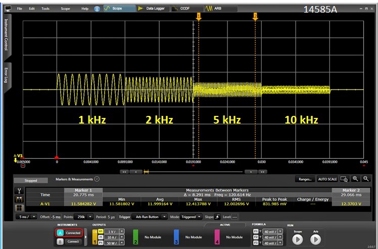
Protect your DUT with power supply features including a watchdog timer

And just last week, on August 20, 2014, my colleague and fellow Watt’s Up? blog contributor, Ed Brorein, presented a live webcast called “Protect Your Device Against Power-Related Damage During Test” which was recorded and can be accessed here. Before he presented the seminar, Ed mentioned it here.

Many of these posts talked about how the power supply responds to an overvoltage or overcurrent condition. Today I want to talk about what causes an overvoltage condition. I’m defining an overvoltage condition as a condition that causes the power supply output voltage to exceed its setting. Let’s take a look at some of the things that can cause this to happen.

Causes of power supply output voltage exceeding its setting

User-caused miswires
These miswires should be found and corrected during test setup verification before a device under test (DUT) is connected to the power supply. Possible miswires and their effect on the power supply output voltage are:

  • Shorted sense leads – the output voltage will rapidly rise above the setting. Keysight power supplies will prevent the output from rising above the overvoltage protection (OVP) setting.
  • Reversed sense leads – on most power supplies, the output voltage will rapidly rise above the setting and on Keysight supplies, it will be stopped by the OVP circuit. On our N6900/N7900 Advanced Power System (APS) power supplies, this condition is caught sooner: OV- is triggered when the output reaches about 10% of the rated voltage, so the output does not have to rise to the setting and above.
  • Open sense leads – If your power supply does not have protection for open sense leads, it is possible for your output to rapidly rise above the setting if one or both sense leads are open. Keysight power supplies have built-in sense protect resistors which limit the output voltage rise to about 1% above the setting. The voltage will continue to be regulated there. In addition to limiting the output to about 1% above the setting with an open sense lead, Keysight N6900/N7900 APS power supplies have a feature called open sense lead detection. When enabled, open sense lead detection will cause a sense fault (SF) status about 50 us after open sense leads are detected. This status does not turn off the output, but it can be configured to turn off the output using the advanced signal routing capability.
  • Special note about N7900 power supplies (not N6900): these models have output disconnect relays that open upon a protection fault. These mechanical relays take about 20 ms to open. Before they open, the output downprogrammer circuit is activated for about 2 ms and draws about 10% of rated output current to reduce the output voltage. The N7976A and N7977A (both higher voltage models) also have solid state relays in series with the mechanical relays. Upon a protection fault on these 2 models, the downprogrammer activates for 2 ms followed immediately by the solid state relays opening and then the mechanical relays open about 20 ms later.
Inadvertent wiring failure
  • Sense leads inadvertently become shorted – power supply response is the same as mentioned above under shorted sense leads
  • Sense leads inadvertently become open – power supply response is the same as mentioned above under open sense leads
  • Sense leads should never become inadvertently reversed, nevertheless, the power supply response is the same as mentioned above under reversed sense leads

Power supply fault (circuit failure)
Note that Keysight’s overall power supply failure rate is very low. Since the below mentioned failures are a subset of all failures, they are very rare. This means that failures that cause the output to go to a higher-than-desired value are a small percent of a small percent, and while not impossible, they are extremely unlikely events.
  • Power element fails (shorts)
    • Series regulator – when a series regulator power element shorts, the output very quickly rises above the rated voltage of the power supply. The only way to limit this is to trip OVP and either fire an SCR across the output to bring the voltage back down or open output relays. For example, the Keysight N678xA models use a series regulator. When OVP trips on N678xA models, output relays are opened to protect the DUT. Solid state relays very quickly open first followed by mechanical relays about 6 ms later.
    • Switching regulator – when a Keysight switching regulator power element shorts, the output will go toward zero volts instead of rising since Keysight switching regulators use power transformers and no power can be transferred through the transformer without the switching elements turning on and off. For example, all N6700 and N6900/N7900 series models use switching regulators except the N678xA models (series regulators).
    • Note that if a power element fails open using either power regulation scheme, the output voltage will fall, not rise, so this condition is not a concern when looking at excessive output voltage possibilities.
  • Regulation circuit failure (bias supply, DAC, amplifier, digital comparison processor, etc.)
    • There are various circuits that could fail and cause the output voltage to rise in an uncontrolled manner. Keysight power supplies have OVP designed to respond to these failures. In series regulators, an SCR across the output can fire to reduce the voltage or output relays can open. In switching regulators, the pulse width modulator is turned off to prevent power from flowing to the output, downprogrammers are activated to pull any excessive voltage down, and output relays are opened (when present) to disconnect the output from the DUT.
    • Multiple parallel failures – if both a regulating circuit fails that causes the output to rise AND the OVP circuit fails, there would be nothing to prevent the output voltage from rising above the setting. While this is possible, it requires just the right combination of multiple circuit failures and is therefore extremely unlikely.
Output response to load current transients
  • It is possible for the output voltage to temporarily rise above the setting for short transients in response to fast load current changes (especially unloading). If the voltage excursion is high enough and long enough, it is possible that the OVP will activate and respond as outlined above.

External power source
  • It is possible for an external source of power (such as a battery, charged capacitor, inductor with changing current, or another power supply) to cause the voltage to go above the setting. The OVP will respond to this condition as outlined above. If the external power source can provide more current than the rating of the power supply and an SCR circuit is used in the power supply, it is prudent to put a fuse in series with the external source of power to prevent damage to the power supply SCR and/or output circuit from excessive current.
So you can see that there are a number of ways in which the output voltage can rise above the setting. Luckily, Keysight design engineers are aware of these possibilities and have lots of experience adding protection circuits to prevent damage to your DUT!

Wednesday, August 20, 2014

Some differences between constant current (CC) and constant resistance (CR) loading on your DUT’s performance

Most electronic loads provide constant current (CC), constant resistance (CR) and constant voltage (CV) loading. Some also offer constant power (CP) loading as well. The primary reason for this is this gives the test engineer a choice of loading that best addresses the loading requirement for the DUT, which invariably is some kind of power source.

Most usually the device should be tested with a load that reflects what the loading is like for its end use. In the most common case of a device being predominantly a voltage source the most common loading choices are either CC or CR loading, which we will look at in more detail here. Some feel they can be used interchangeably when testing a voltage source. To some extent this is true but in some cases only one or the other should be used as they can impact the DUT’s performance quite differently.

Let’s first consider static performance. In Figure 1 we have the output characteristics of an ideal voltage source with zero output resistance (a regulated power supply, for example) and a non-ideal voltage source having series output resistance (a battery, for example).  Both have the same open circuit (no load) voltage. Superimposed on these two source output characteristics are two load lines; one for CC and one for CR. As can be seen they are set to draw the same amount of current for the ideal voltage source. However, for the non-ideal voltage source, while the CC load still continues to draw the same amount of current in spite of the voltage drop, not surprisingly the CR load draws less current due to its voltage-dependent nature.


Figure 1: CC and CR loading of ideal and non-ideal voltage sources

CC loading is frequently used for static power supply tests for a key reason. Power supplies are usually specified to have certain output voltage accuracy for a fixed level of current. Using CC loading assures the loading condition is met, regardless of power supply’s output voltage being low or high, or in or out of spec. Non-ideal voltage sources, like batteries, present a little more of a problem and are often specified for both CC and CR loading as a result, to reflect the nature of the loading they may be subjected to in their end use. Due to a battery's load-dependent output voltage, trying to use one type of loading in place the other becomes an iterative process of checking and adjusting loading until the acceptable operating point is established.

Let’s now consider dynamic performance.  CC loading generally has a greater impact on a power supply’s ability to turn on as well as its transient performance and stability, in comparison to CR loading. When the power supply first starts up its output voltage is at zero. A CR load would demand zero current at start up. In comparison a CC load still demands full current. Some power supplies will not start up properly under CC loading. With regard to transient response and stability, CR loading provides a damping action, increasing current demand when the transient voltage increases and decreases demand when the transient voltage decreases, because the current demand is voltage dependent. CC loading does not do this, which can negatively influence transient response and stability somewhat. Whether CC or CR loading is used depends on what the power supply’s specifications call out for the test conditions. Batteries have some dynamic considerations as well. Their output response can be modeled as a series of time constants spanning a wide range of time. This presents somewhat of a moving target for an algorithm that uses an iterative approach to settling on an acceptable operating point.


This is just a couple of examples of how a load’s characteristic affects the performance of the device it is loading, and why electronic loads have multiple operating modes to select from, and worth giving thought next time towards how your device is affected by its loading!

Tuesday, August 5, 2014

Upcoming Seminar on Protecting Your Device against Power-Related Damage during Test

Here on “Watt’s Up?” we have provided a good number of posts about various protection features incorporated into system power supplies to protect your device against power-related damage during test. Just recently my colleague Gary posted “How Does Power Supply Over-Voltage Work?” (Click here to review) Here he reviews inner workings of different OVP implementations.  I recently posted “Safeguarding Your Power-Sensitive DUTs against an Over-Power Condition” (Click here to review) Here I go over a method to protect your DUT against excess power when other power supply features like over current protection may be less than ideal.

The reason why we frequently share power-related protection topics here is protecting your DUT is extremely important, there are a lot of different capabilities incorporated in system power supplies for this purpose, and there are a lot of practical considerations when putting them to use.  

Hopefully a number of you have found our posts on protection-related topics of help. Because this is a very important topic and there is so much more you should know about it I will be giving a live web-based seminar “Protecting Your Device against Power-Related Damage during Test” on August 20th, just a few weeks away from today. I will be going over a number of protection-related topics which we have not yet covered here on “Watt’s Up?”.  One of my objectives is to provide a more holistic view of the many ways a system power supply is able to better safeguard against power-related damage as well as what is practical to expect when using these various capabilities incorporated in the power supply.

You can register online at the following (Click here for description and registration page) In case you are not able to attend the live event on August 20 you will be able to register and listen to seminar afterward as well, as it will be recorded.


So if protecting your device against power-related damage is important to you I hope you are able to attend the seminar!

Thursday, July 31, 2014

Using an IVI Class Compliant Driver

Hi everybody!

In the past, I have talked about the different driver options that we offer.  One of them is the IVI-COM/IVI-C driver.  IVI actually stands for Interchangeable Virtual Instruments. Today I am going to talk about how you can make that abbreviation true using the fact that our power supply can use the IviDCPwr class.   I have received  a few questions in the past about how to do this and every time I do it, it takes me a while to remember all of the steps.  Posting it here will put it somewhere where people (including me!) can find it easily

To start off you need to download and install the following:
  • The Agilent N6700 IVI-COM/IVI-C  driver from Agilent’s website.  If you get the driver from somewhere else, I am not sure how it will work.
  • NI VISA since you will need NI-MAX
  • IVI Compliance package

Once you have all of this, you are ready to get started.


The first thing that you need to do is set your targeted instrument in NI-MAX.  I have a N6702A connected to my LAN.  Here's how it shows up in MAX:


After that, you want to go to the "IVI-Drivers" menu, select the "Driver Sessions" item and right click on it to select "Create new".   From there, click on the "software" tab and select the appropriate driver, in this case the AgN67xx driver.  


You can see here that the driver complies to the IviDcpwr class whcih is what we will be using.  

The next thing to do is in the "Hardware" Tab of the same menu.  You need to specify which instruments use this driver.  Click on "Add" to add your instrument.  It should look like this:


 One thing that I cannot stress enough is that you need to check that checkbox.  In you don't, this will not work and you will spend a little bit of time trying to figure out why you are getting resource not found errors.  Believe me I know this from experience!  After you double check everything make sure that you click on "Save IVI Configuration".

Now choose "Logical Names".  Right click on it and select "Create New".  I created a logical name called "MPS" (this stands for Modular Power System if you were wondering).  You need to refer it to the correct driver session:


Make sure to click on "Save IVI Configuration" again.

With that, you are ready to actually start!  I used Visual C++ 2010 to write my example.  Make sure that you have all of the IVI directories properly entered in your project.  Also make sure that you reference the ividcpwr.lib file in your "linker" settings. 

Here is my program listing:

#include <stdio.h>
#include "IviDCPwr.h"

void main()
{
ViStatus status;
ViSession session;
ViRsrc resource = "MPS";
ViConstString options  = "QueryInstrStatus=true, Simulate=false, DriverSetup= Model=, Trace=false";
ViBoolean idQuery = VI_FALSE;
ViBoolean reset   = VI_TRUE;
ViBoolean enabled = VI_TRUE;
ViChar ChannelName[16] = "";
        ViInt32 index = 2;
        ViInt32 bufferSize = 256;
ViConstString Cname;
ViReal64 Vmeasurement;
ViReal64 Ameasurement;

// This program initializes a session, programs a voltage and current on channel 2, 
// enables the output, and measures voltage and current.

status = IviDCPwr_InitWithOptions(resource, idQuery, reset, options, &session);
status = IviDCPwr_GetChannelName (session,index, bufferSize,ChannelName);

Cname = ChannelName;

status = IviDCPwr_ConfigureOutputEnabled (session,Cname,enabled);
status = IviDCPwr_ConfigureVoltageLevel (session,Cname,4.0);
status = IviDCPwr_ConfigureCurrentLimit(session, Cname, IVIDCPWR_VAL_CURRENT_TRIP, 1);

status = IviDCPwr_Measure (session,Cname,IVIDCPWR_VAL_MEASURE_VOLTAGE,&Vmeasurement);
printf("Measured Voltage on channel is : %f V \n",Vmeasurement);

status = IviDCPwr_Measure (session,Cname,IVIDCPWR_VAL_MEASURE_CURRENT,&Ameasurement);
printf("Measured Current on channel is : %f A \n",Ameasurement);

status = IviDCPwr_close (session);

printf("\n Done - Press Enter to Exit");
getchar();  
}

I am not going to go over the program in detail but here are the key things to note:
  • You need to include "IviDCPwr.h".  All the functions are in there.  You do not need to reference the instrument specific driver.
  • When you initialize the unit, you can refer to it by the name that you define in the "Logical Names" tab above.  In my case, I use "MPS".
  • This is a modular power supply.  The variable "index" is controlling the channel.  
  • I have tested this program and it works properly.
In theory, you should be able to swap this power supply out with another class compliant power supply with minimal programming changes (though in this case if you switch to a single output supply you would need to take out the references to the multiple channels).

One last thing that I want to note is that this will be the last Watt's Up blog posted under the Agilent banner.  Don't worry, we will still be posting the same great content but it will be under a Keysight Technologies banner.  I have been working for Agilent for 14 years now so it will be odd at first to have a new name but I am looking forward to posting many more blogs as a Keysight employee.  Goodbye Agilent Technologies it's been an interesting 14 years!


Wednesday, July 30, 2014

How does power supply overvoltage protection work?

In past posts, I’ve written about what overvoltage protection (OVP) is (click here), where it is sensed (click here), and its history (click here). Today I want to cover a little about how it works inside the power supply.

As a quick review, OVP is a built-in power supply feature that protects the device under test (DUT) from excessive voltage by shutting down the power supply output if it senses voltage that exceeds the OVP setting. Depending on the power supply design, the voltage may be sensed at the output terminals or at the sense terminals.

Most of Agilent’s older power supplies sense OVP at the output terminals and use a simple analog comparator circuit to determine when the output exceeds the OVP threshold set by the user. The OVP threshold is translated into an overvoltage reference voltage (OVref) that could come from a simple divider with a potentiometer for adjustment (uncalibrated and rather crude) or from a more sophisticated calibrated digital-to-analog converter (DAC) voltage. When the comparator sees the scaled output voltage exceed the OVref voltage, the overvoltage trip (OVtrip) signal is generated which shuts down the power supply output and, on some designs, fires an SCR across the output. See Figure 1 for a simplified representation of this arrangement.

Some of our newer designs look for an overvoltage condition on the sense terminals for better accuracy. In this scheme, the sense voltage feeds one comparator input through a differential amplifier while the other comparator input is driven by the user-set calibrated OVref voltage. See Figure 2. An output terminal OVP as described above must also be used as a backup with these designs (not shown in Figure 2) because some OV conditions are not caught when sensing OV on the sense terminals. For example, if the sense leads are shorted together, the output voltage will go up uncontrolled yet the sense voltage will remain at zero volts.

Some other OVP designs use a calibrated analog-to-digital converter (ADC) on either the output terminal voltage or the sense terminal voltage and compare the measured digital data to the user’s threshold setting. See Figure 3. To avoid nuisance OVP shutdowns, this scheme frequently requires several analog-to-digital conversions in a row exceed the threshold (for example, 4). This adds a minor delay to the OVP response time. With fast ADC conversion rates, the OVP response can still be just a few tens of microseconds and it is worth spending a little extra time to gain immunity against nuisance tripping. For example, the Agilent N6781A uses this technique. Since it does an ADC conversion every 5 us and requires 4 consecutive conversions exceed the OVP threshold to cause a shutdown, it will trip in less than 30 us.

So you can see that there are various ways to implement overvoltage protection. In all cases, rest assured that your DUT is protected against excessive voltage when using Agilent power supplies!

Tuesday, July 22, 2014

What does it mean when my Agilent power supply displays “Osc”?

When using certain higher performance power supplies from Agilent, like the N678xA series source-measure modules, you may discover that the output has shut down and an annunciator displaying “Osc” shows up on the front panel meter display, like that shown in Figure 1 for the N6705B DC Power Analyzer mainframe. 


Figure 1: DC Power Analyzer front panel meter displaying “Osc” on channel 1 output

As you would likely guess, Osc stands for oscillation and this means the output has been shut down for an oscillation fault detection. In this particular instance an N6781A high performance source measure module was installed in channel 1 of the N6705B DC Power Analyzer mainframe.

The N678xA series source measure modules have very high bandwidth so that they can provide faster transient response and output slew rates. However, when the bandwidth of the power supply is increased, its output stability becomes more dependent on the output wiring and DUT impedances. To provide this greater bandwidth and at the same time accommodate a wider range of DUTs on the N678xA modules, there are multiple compensation ranges to select from, based on the DUT’s input capacitance, as shown in the advanced source settings screen in Figure 2.


Figure 2: DC Power Analyzer front panel displaying advanced source settings for the N678xA

Note that “Low” compensation range supports the full range of DUT loading capacitance but this is the default range. While it provides the most robust stability, it does not have the faster response and better performance of the “High” compensation ranges.

As long as the wiring to the DUT is correctly configured and an appropriate compensation range is selected the output should be stable and not trip the oscillation protection system. In the event of conditions leading to an unstable condition, any detection of output oscillations starting up quickly shut down the output in the manner I captured in Figure 3. I did this by creating an instability by removing the load capacitance.


Figure 3: Oscillation protection being tripped as captured in companion 14585A software

In rare circumstances, such as with some DUTs drawing extremely high amplitude, high frequency load currents, which may lead to false tripping, the oscillation protection can be turned off, as shown in Figure 4.


Figure 4: N678xA oscillation protection disable in N6705B DC Power Analyzer advance protection screen

Oscillation protection is a useful mechanism that can protect your DUT and your power supply from an excessively high AC voltage and current due to unstable operating conditions. Now you know what it means next time you see “Osc” displayed on the front panel of you Agilent power supply and what you need to do to rectify it!

.

Monday, July 14, 2014

Extending the usable bandwidth of the DC source when performing AC disturbance testing on your DUT

A lot of various products that run off of DC power, often destined to be used in automobiles and other types of vehicles, but even quite a number in stationary applications as well, require validation testing for impact of having AC disturbances riding on top the DC powering them.

 Conducting this type of testing is often a big challenge for the test engineer in finding a solution that adequately addresses the disturbance test requirements. It usually requires multiple pieces of hardware:
  • A DC power supply is used to provide the DC bias voltage and power.
  • A power amplifier is used to generate the AC disturbance.
  • A separate ARB /function generator is needed to produce the reference signal for the disturbance

Coupling the DC power supply and power amplifier together is extremely problematic. While it would be great to just directly connect the two in series, this rarely can be done in practice as the power amplifier usually cannot handle the DC current of the power supply. A variety of custom approaches are then typically taken, all with their associated drawbacks.

An article about this very topic was published last year, written by a colleague I work with, Paul Young in our R&D group. As he noted it’s great when the power source can provide both the DC power as well as the AC disturbance as this is a big savings over trying to incorporate multiple pieces of equipment. Paul’s article “Extending the Usable Bandwidth of a Programmable Power Supply for Generating Sinusoidal Waveforms” (click here to review) is an excellent reference on this and the inspiration for my blog posting this week.

Our N6705B DC Power Analyzer in Figure 1 and recently introduced N7900A series Advanced Power System (APS) 1KW and 2KW power supplies in Figure 2 have proven to be very useful for doing a variety of testing where transients and audio disturbances are needing to be introduced on top of the DC that is powering the DUT.


Figure 1: Agilent N6705B DC Power Analyzer and N6700 series DC power modules


Figure 2: Agilent N7900A series 1KW and 2KW Advanced Power System and N7909A Power Dissipator

The reasons for these products being useful for disturbance testing are due to their built in ARB generation capability in conjunction with having a respectable AC bandwidth, on top of being able to source the DC power. Everything can be done within one piece of equipment.

A very common test need is to superimpose a sinusoidal disturbance in the audio range. One example of this is in automobiles. The alternator “whine” AC ripple induced on top of the DC output falls within this category. Our 1KW and 2KW N7900A series APS are good for applications needing higher DC power. However, at first glance the specified AC bandwidth of 2 kHz on does not look like it would work well for higher audio frequencies. The AC response of an N7951A from 1 kHz to 10 kHz is shown in Figure 3. This was captured using the 14585A companion software to set up its ARB.  There is noticeable roll off for higher frequency, as expected.


Figure 3: N7951A APS AC response characteristics captured using companion 14585A software

However, it’s worth noting that the roll off is gradual and very predictable. In the case of superimposing a relatively small AC signal on top of the DC output it is easy to compensate by measuring the attenuation at the given frequency and applying a gain factor to correct for it, as I did as shown in Figure 4. As one example, for 5 kHz, I programmed 2.38 volts peak to get the desired 1 volt peak.


Figure 4: N7951A APS AC response characteristics after gain correction

As can be seen it was simple to now get a flat response over the entire range. A limiting factor here is sum of the programmed DC value plus programmed AC peak value needs to be within the voltage programming range of the power supply being used. In practice, when the AC disturbance is reasonably small it is easy to cover a wide range of frequency.

Another factor to consider is capacitive loading. Some DC powered products sometimes have a fairly substantial filter capacitor built in across the DC power input. This will increase the peak current drain from the power supply when AC is applied on top of the DC. As an example a 100 microfarad capacitor will draw a peak current of 6.28 amps when a 10 kHz, 1 volt peak AC signal is applied. There may also be series impedance limiting the peak current, but whatever this AC peak current is it needs to be included when determining the size of the power supply needed.

With these basic considerations you will be able to perform AC disturbance testing over a much greater bandwidth as well!

.