Showing posts with label disturbance testing. Show all posts

Monday, October 6, 2014

Simulating battery contact bounce, part 2

In part 1 of this posting on simulating battery contact bounce (click here to review) I discussed what battery contact bounce is about and why creating a voltage dropout may not be adequate for simulating battery contact bounce. The first answer to addressing this was provided; use a blocking diode and then a voltage dropout is certain to be suitable for simulating battery contact bounce.

Another approach for simulating battery contact bounce is to add a solid state switch between the DC source and the battery powered device. While this is a good approach it is complex to implement. A suitable solid state switch needs to be selected along with coming up with an appropriate way to power and drive the input of the switch need to be developed.

If for some reason using a blocking diode is not suitable, there is yet another fairly simple approach that can be taken to simulate high impedance battery contact bounce. Instead of programming a voltage dropout on the DC source, program a current dropout. Where the voltage going to zero during a voltage dropout is effectively a short circuit, as we saw in part 1, the current going to zero during a current dropout is effectively an open circuit. There are a couple of caveats for doing this. The main one is battery powered devices are powered from a battery, which is a voltage source, not a current source. In order for the DC source to act as a voltage source when delivering power, we need to rely on the DC source voltage limit being set to the level of the battery voltage. In order for this to happen we need to set the non-dropout current level to be in excess of the maximum level demanded by the device being powered and. Thus the DC source will normally be operating in voltage limit. Then when the current dropout drives the output current to zero, the DC source switches its operating mode from voltage limit to constant 
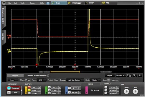
current, with a current value of zero. This operation is depicted in Figure 4, using a Keysight N6781A 2-quadrant SMU module designed for testing battery powered devices, operating within an N6705B DC Power Analyzer. In this example the current ARB for the dropout was both programmed and the results shown in Figure 1 captured using the companion 14585A software.


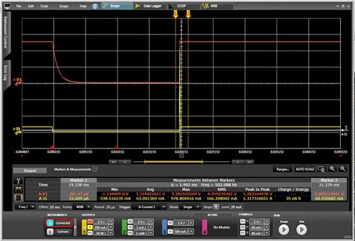
Figure 1: Current ARB creates a high impedance dropout to simulate battery contact bounce

Another caveat with using this approach for simulating battery contact bounce is paying careful attention to the behavior of the mode crossovers. For the first crossover, from voltage limit to constant current operation (at zero current) there is a small amount of lag time, typically just a fraction of a millisecond, before the transition happens. This becomes more significant only when trying to simulate extremely short contact bounce periods. More important is when crossing back over from constant zero current back to voltage limit operation. There is a short period when the current goes up to its high level before the voltage limit gains control, holding the voltage at the battery’s voltage level. Usually any capacitance at the input of the DUT will normally absorb any short spike of current. If this crossover is slow enough, and there is very little or no capacitance, the device could see a voltage spike. The N6781A has very fast responding circuits however, minimizing crossover time and inducing just 250 mV of overshoot, as is seen in Figure 1.

Hopefully, now armed with all of these details, you will be able to select an approach that works best for you for simulating battery contact bounce!


Wednesday, September 17, 2014

Simulating battery contact bounce, part 1

One test commonly done during design validation of handheld battery powered devices is to evaluate their ability to withstand a short loss of battery power due to being bumped and the contacts momentarily bouncing open, and either remain operating or have sufficient time to handle a shutdown gracefully. The duration of a contact bounce can typically range anywhere from under a millisecond to up to 100 milliseconds long.

To simulate battery contact bouncing one may consider programming a voltage drop out on a reasonably fast power supply with arbitrary waveform capabilities, like several of the N675xA, N676xA, or N678xA series modules used in the N6700 series Modular DC Power System or N6705B DC Power Analyzer mainframe, shown in Figure 1. It is a simple matter to program a voltage dropout of specified duration. As an example a voltage dropout was programmed in Figure 2 on an N6781A SMU module using the companion 14585A software.


 Figure 1: N6700 series and N6705B mainframes and modules


Figure 2: Programming a voltage drop out using the N6705B and N6781A SMU module

While a voltage dropout is fine for many applications, like automotive, in many situations it does not work well for simulating battery contact bounce. The reason for this is there is one key difference to note about a voltage dropout versus a battery contact bounce. During a voltage dropout the source impedance remains low. During a battery contact bounce the source impedance is an open circuit. However, a DC source having the ability to generate a fast voltage dropout is a result of it being able to pull its output voltage down quickly. This is due to its ability to sink current as well as source current. The problem with this is, for many battery powered devices, this effectively short-circuits the battery input terminals, more than likely causing the device to instantly shut down by discharging any carry-over storage and/or disrupting the battery power management system. As one example consider a mobile device having 50 microfarads of input capacitance and draws 4 milliamps of standby current. This capacitance would provide more than adequate carryover for a 20 millisecond battery contact bounce. However, if a voltage dropout is used to simulate battery contact bounce, it immediately discharges the mobile device’s input capacitance and pulls the battery input voltage down to zero, as shown by the red voltage trace in Figure 3. The yellow trace is the corresponding current drain. Note the large peaks of current drawn that discharge and recharge the DUT’s input capacitor.


 Figure 3: Voltage dropout applied to DUT immediately pulls voltage down to zero

One effective solution for preventing the DC source from shorting out the battery input is to add a DC blocking diode in series with the battery input, so that current cannot flow back out, creating high impedance during the dropout. This is illustrated in Figure 4.


Figure 4: Blocking diode added between SMU and DUT

One thing to note here is the diode’s forward voltage drop needs to be compensated for. Usually the best way to do this just program the DC source with the additional voltage needed to offset the diode’s voltage drop. The result of this is shown in Figure 5. As shown by the red trace the voltage holds up relatively well during the contact bounce period. Because the N6781A SMU has an auxiliary voltage measurement input it is able to directly measure the voltage at the DUT, on the other side of the blocking diode, instead of the output voltage of the N6781A. As seen by the yellow current trace there is no longer a large peak of current discharging the capacitor due to the action of the blocking diode.


 Figure 5: Blocking diode prevents voltage dropout from discharging DUT 

Now you should have a much better appreciation of the differences between creating a voltage dropout and simulating battery contact bounce! And as can be seen a blocking diode is a rather effective means of simulating battery contact bounce using a voltage dropout. Stay tuned for my second part on additional ways of simulating battery contact bounce on an upcoming posting.
.


Monday, July 14, 2014

Extending the usable bandwidth of the DC source when performing AC disturbance testing on your DUT

A lot of various products that run off of DC power, often destined to be used in automobiles and other types of vehicles, but even quite a number in stationary applications as well, require validation testing for impact of having AC disturbances riding on top the DC powering them.

 Conducting this type of testing is often a big challenge for the test engineer in finding a solution that adequately addresses the disturbance test requirements. It usually requires multiple pieces of hardware:
  • A DC power supply is used to provide the DC bias voltage and power.
  • A power amplifier is used to generate the AC disturbance.
  • A separate ARB /function generator is needed to produce the reference signal for the disturbance

Coupling the DC power supply and power amplifier together is extremely problematic. While it would be great to just directly connect the two in series, this rarely can be done in practice as the power amplifier usually cannot handle the DC current of the power supply. A variety of custom approaches are then typically taken, all with their associated drawbacks.

An article about this very topic was published last year, written by a colleague I work with, Paul Young in our R&D group. As he noted it’s great when the power source can provide both the DC power as well as the AC disturbance as this is a big savings over trying to incorporate multiple pieces of equipment. Paul’s article “Extending the Usable Bandwidth of a Programmable Power Supply for Generating Sinusoidal Waveforms” (click here to review) is an excellent reference on this and the inspiration for my blog posting this week.

Our N6705B DC Power Analyzer in Figure 1 and recently introduced N7900A series Advanced Power System (APS) 1KW and 2KW power supplies in Figure 2 have proven to be very useful for doing a variety of testing where transients and audio disturbances are needing to be introduced on top of the DC that is powering the DUT.


Figure 1: Agilent N6705B DC Power Analyzer and N6700 series DC power modules


Figure 2: Agilent N7900A series 1KW and 2KW Advanced Power System and N7909A Power Dissipator

The reasons for these products being useful for disturbance testing are due to their built in ARB generation capability in conjunction with having a respectable AC bandwidth, on top of being able to source the DC power. Everything can be done within one piece of equipment.

A very common test need is to superimpose a sinusoidal disturbance in the audio range. One example of this is in automobiles. The alternator “whine” AC ripple induced on top of the DC output falls within this category. Our 1KW and 2KW N7900A series APS are good for applications needing higher DC power. However, at first glance the specified AC bandwidth of 2 kHz on does not look like it would work well for higher audio frequencies. The AC response of an N7951A from 1 kHz to 10 kHz is shown in Figure 3. This was captured using the 14585A companion software to set up its ARB.  There is noticeable roll off for higher frequency, as expected.


Figure 3: N7951A APS AC response characteristics captured using companion 14585A software

However, it’s worth noting that the roll off is gradual and very predictable. In the case of superimposing a relatively small AC signal on top of the DC output it is easy to compensate by measuring the attenuation at the given frequency and applying a gain factor to correct for it, as I did as shown in Figure 4. As one example, for 5 kHz, I programmed 2.38 volts peak to get the desired 1 volt peak.


Figure 4: N7951A APS AC response characteristics after gain correction

As can be seen it was simple to now get a flat response over the entire range. A limiting factor here is sum of the programmed DC value plus programmed AC peak value needs to be within the voltage programming range of the power supply being used. In practice, when the AC disturbance is reasonably small it is easy to cover a wide range of frequency.

Another factor to consider is capacitive loading. Some DC powered products sometimes have a fairly substantial filter capacitor built in across the DC power input. This will increase the peak current drain from the power supply when AC is applied on top of the DC. As an example a 100 microfarad capacitor will draw a peak current of 6.28 amps when a 10 kHz, 1 volt peak AC signal is applied. There may also be series impedance limiting the peak current, but whatever this AC peak current is it needs to be included when determining the size of the power supply needed.

With these basic considerations you will be able to perform AC disturbance testing over a much greater bandwidth as well!

.