Showing posts with label N6705B DC Power Analyzer. Show all posts

Wednesday, July 29, 2015

Battery drain test on anniversary gift clock

Last month, on June 2, 2015, I celebrated working for Hewlett-Packard/Agilent Technologies/Keysight Technologies for 35 years. During the earlier times of my career, on significant anniversaries such as 10 years or 20 years, employees could choose from a catalog of gifts to have their contributions to the company recognized. That tradition has been discontinued, but I did select a couple of nice gifts over the years. During my HP days, one gift I selected was a clock with a stand shown here:
I have had that clock for decades and it uses a silver oxide button cell battery (number 371). I have to replace the battery about once per year and wondered if that made sense based on the battery capacity and the current drain the clock presents to the battery. I expected the battery to last longer so I wanted to know if I was purchasing inferior batteries. These 1.5 V batteries are rated for about 34 mA-hours. So I set out to measure the current drain using our N6705B DC Power Analyzer with an N6781A 2-Quadrant Source/Measure Unit for Battery Drain Analysis power module installed. Making the measurement was simple…..making the connections to the tiny, delicate battery connection points was the challenging part. After one or two failed attempts (I was being very careful because I did not want to damage the connections), I solicited the help of my colleague, Paul, who handily came up with a solution (thanks, Paul!). Here is the final setup and a close-up of the connections:


I set the N6781A voltage to 1.5 V and used the N6705B built-in data logger to capture current drawn by the clock for 5 minutes, sampling voltage and current about every 40 us. The clock has a second hand and as expected, the current showed pulses once per second when the second hand moved (see Figure 1). Each current pulse looks like the one shown in Figure 2. There was an underlying 200 nA being drawn in between second-hand movements. All of this data is captured and shown below in Figure 3 showing the full 5 minute datalog along with the amp-hour measurement (0.28 uA-hours) and average current measurement (3.430 uA) between the markers.


Given the average current draw, I can calculate how long I would expect a 34 mA-hour battery to last:

                 34 mAh / 3.430 uA average current = 9912.54 hours = about 1.13 years

This is consistent with me changing the battery about every year, so once again, all makes sense in the world of energy and electronics (whew)! Thanks to the capabilities of the N6705B DC Power Analyzer, I now know the batteries I’m purchasing are lasting the expected time given the current drawn by the clock. How much current is your product drawing from its battery?

Wednesday, July 15, 2015

Optimizing the performance of the zero-burden battery run-down test setup

Two years ago I added a post here to “Watt’s Up?” titled:  “Zero-burden ammeter improves battery run-down and charge management testing of battery-powered devices” (click here to review). In this post I talk about how our N6781A 20V, 3A 20W SMU (and now our N6785A 20V, 8A, 80W as well) can be used in a zero-burden ammeter mode to provide accurate current measurement without introducing any voltage drop. Together with the independent DVM voltage measurement input they can be used to simultaneously log the voltage and current when performing a battery run-down test on a battery powered device. This is a very useful test to perform for gaining valuable insights on evaluating and optimizing battery life. This can also be used to evaluate the charging process as well, when using rechargeable batteries. The key thing is zero-burden current measurement is critical for obtaining accurate results as impedance and corresponding voltage drop when using a current shunt influences test results. For reference the N678xA SMUs are used in either the N6705B DC Power Analyzer mainframe or N6700 series Modular Power System mainframe.
There are a few considerations for getting optimum performance when using the N678xA SMU’s in zero-burden current measurement mode. The primary one is the way the wiring is set up between the DUT, its battery, and the N678xA SMU. In Figure 1 below I rearranged the diagram depicting the setup in my original blog posting to better illustrate the actual physical setup for optimum performance.

Figure 1: Battery run-down setup for optimum performance
Note that this makes things practical from the perspective that the DUT and its battery do not have to be located right at the N678xA SMU.  However it is important that the DUT and battery need to be kept close together in order to minimize wiring length and associated impedance between them. Not only does the wiring contribute resistance, but its inductance can prevent operating the N678xA at a higher bandwidth setting for improved transient voltage response. The reason for this is illustrated in Figure 2.


Figure 2: Load impedance seen across N678xA SMU output for battery run-down setup
The load impedance the N678xA SMU sees across its output is the summation of the series connection of the DUT’s battery input port (primarily capacitive), the battery (series resistance and capacitance), and the jumper wire between the DUT and battery (inductive). The N678xA SMUs have multiple bandwidth compensation modes. They can be operated in their default low bandwidth mode, which provides stable operation for most any load impedance condition. However to get the most optimum voltage transient response it is better to operate N678xA SMUs in one of its higher bandwidth settings. In order to operate in one of the higher bandwidth settings, the N678xA SMUs need to see primarily capacitive loading across its remote sense point for fast and stable operation. This means the jumper wire between the DUT and battery must be kept short to minimize its inductance. Often this is all that is needed. If this is not enough then adding a small capacitor of around 10 microfarads, across the remote sense point, will provide sufficient capacitive loading for fast and stable operation. Additional things that should be done include:
  • Place remote sense connections as close to the DUT and battery as practical
  • Use twisted pair wiring; one pair for the force leads and a second pair for the remote sense leads, for the connections from the N678xA SMU to the DUT and its battery


By following these best practices you will get the optimum performance from your battery run-down test setup!

Tuesday, June 16, 2015

When is it best to use a battery or a power supply for testing my battery powered device?

As I do quite a bit of work with mobile battery powered devices I regularly post articles here on our “Watt’s Up?” blog about aspects on testing and optimizing battery life for these devices. As a matter of fact my posting from two weeks ago is about the webcast I will be doing this Thursday, June 18th: “Optimizing Battery Run and Charge Times of Today’s Mobile Wireless Devices”. That’s just two days away now!

With battery powered devices there are times it makes sense to use the device’s actual battery when performing testing and evaluation work to validate and gain insights on optimizing performance. In particular you will use the battery when performing a battery run-down test, to validate run-time. Providing you have a suitable test setup you can learn quite a few useful things beyond run-time that will give insights on how to better optimize your device’s performance and run-time. I go into a number of details about this in a previous posting of mine: “Zero-burden ammeter improves battery run-down and charge management testing of battery-powered devices”. If you are performing this kind of work you should find this posting useful.

However, there are other times when it makes sense to use a power supply in place of the device’s battery, to power up the device for the purpose of performing additional types of testing and evaluation work for optimizing the device’s performance. One major factor for this is the power supply can be directly set to specific levels which remain fixed for the desired duration. It eliminates the variability and difficulties of trying to do likewise with a battery, if at all possible. In most all instances it is important that the power supply provides the correct characteristics to properly emulate the battery. This includes:
  • Full two-quadrant operation for sourcing and sinking current and power
  • Programmable series resistance to simulate the battery’s ESR

These characteristics are depicted in the V-I graph in figure 1.


Figure 1: Battery emulator power supply output characteristics

Note that quadrant 1 operation is emulating when the battery is providing power to the device while quadrant 2 is emulating when the battery is being charge by the device.


A colleague here very recently had an article published that goes into a number of excellent reasons why and when it is advantageous to use a power supply in place of trying to use the actual battery, “Simulating a Battery with a Power Supply Reaps Benefits”. I believe you will find this to also be a useful reference.

Wednesday, June 3, 2015

Webcast this June 18th: Optimizing Battery Run and Charge Times of Today’s Mobile Wireless Devices

One thing for certain: Technological progress does not stand still for a moment and there is no place where this is any truer than for mobile wireless devices! Smart phones, tablets, and phablets have all but totally replaced yesterday’s mobile phones and other personal portable devices. They provide virtually unlimited information, connectivity, assistance, and all kinds of other capabilities anywhere and at any time.

However, as a consequence of all these greater capabilities and time spent being actively used is battery run time limitations. Battery run time is one of top dissatifiers of mobile device users. To help offset this manufacturers are incorporating considerably larger capacity batteries to get users through their day. I touched upon this several weeks ago with my earlier posting “Two New Keysight Source Measure Units (SMUs) for Battery Powered Device and Functional Test”. We developed higher power versions of our N678xA series SMUs in support of testing and development of these higher power mobile devices.

Ironically, a consequence of higher capacity batteries leads to worsening of another top user dissatifier, and that is battery charging time. Again, technological progress does not stand still! New specifications define higher power delivery over USB, which can be used to charge these mobile devices in less time. I also touched upon this just a few weeks ago with my posting “Updates to USB provide higher power and faster charging”. The power available over USB will no longer be the limiting factor on how long it takes to recharge a mobile device.

I have been doing a good amount of investigative work on these fronts which has lead me to put together a webcast “Optimizing Battery Run and Charge Times of Today’s Mobile Wireless Devices”. Here I will go into details about operation of these mobile devices during use and charging, and subsequent testing to validate and optimize their performance.  If you do development work on mobile devices, or even have a high level of curiosity, you may want to attend my webinar on June 18. Additional details about the webcast and registration are available at: “Click here for accessing webcast registration”. I hope you can make it!


Wednesday, March 11, 2015

Comparing effects of using pulsed and steady state power to illuminate a high brightness LED

I was having a discussion here with a colleague about the merits of powering a high brightness LED (HBLED) using pulsed power versus using steady state DC power.

My opinion was: “Basically, amperes in proportionally equates to light flux out, so you will get about the same amount of illumination whether it is pulsed or DC.”

His argument was: “Because the pulses will be brighter, it’s possible the effective illumination that’s perceived will be brighter. Things appear to be continuous when discrete fixed images are updated at rates above thirty times a second, and that should apply to the pulsed illumination as well!”

I countered: “It will look the same and, if anything, will be less efficient when pulsed!”

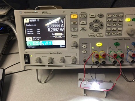
So instead of continuing our debate we ran a quick experiment. I happened to have some HBLEDs so I hooked one up to an N6781A DC source measure module housed in an N6705B DC Power Analyzer sitting at my desk, shown in Figure 1. The N6781A has excellent current sourcing characteristics regardless whether it is DC or a dynamic waveform, making it a good choice for this experiment.


Figure 1: Powering up an HBLED

First we powered it up with a steady state DC current of 100 mA. At this level the HBLED had a forward voltage drop of 2.994 V and resulting power of 0.2994 W, as seen in Figure 2, captured using the companion 14585A control and analysis software.


Figure 2: Resulting HBLED voltage and power when powered with 100 mA steady state DC current

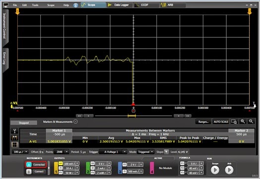
We then set the N6781A to deliver a pulsed current of 200 mA with a 50% duty cycle, so that its average current was 100 mA. The results were again captured using the 14585A software, as shown in Figure 3.


Figure 3: Resulting HBLED voltage and power when powered with 200 mA 50% DC pulsed current

Switching back and forth between steady state DC and pulsed currents, my colleague agreed, the brightness appeared to be comparable (just as I had expected!).  But something more interesting to note is the average current, voltage, and power. These values were obtained as shown in Figure 3 by placing the measurement markers over an integral number of waveform cycles. The average current was 100 mA, as expected. Note however that the average voltage is lower, at 2.7 V, while the average power is higher, at 0.3127 W! At first the lower average voltage together with higher average power would seem to be a contradiction. How can that be?

First, in case you did not notice, the product of the RMS voltage and RMS current are 0.3897 W which clearly does not match our average power value displayed. What, another contradiction? Why is that? Multiplying RMS voltage and RMS current will give you the average power for a linear resistive load but not for a non-linear load like a HBLED. The average power needs to be determined by taking an overall average of the power over time computed on a point-by-point basis, which is how it is done within the 14585A software as well as within our power products that digitize the voltage and current over time. Second, the average voltage is lower because it drops down towards zero during periods of zero current. However it is greater during the periods when 200 mA is being sourced through the HBLED and these are the times where power is being consumed.

So here, by using pulsed current, our losses ended up being 4.4% greater when powered by the comparable steady state current. These losses are mainly incurred as a result of greater resistive drop losses in the HBLED occurring at the higher current level.

There is supposed to be one benefit however of using pulsed power when powering HBLEDs. At different steady state DC current levels there is some shift in their output light spectrum. Using pulsed current provides dimming control while maintaining a constant light spectrum. This prevents minor color shifts at different illumination levels. Although I would probably never notice it!

Tuesday, February 24, 2015

Two New Keysight Source Measure Units (SMUs) for Battery Powered Device and Functional Test

Over the past few years here on “Watt’s Up?” I have posted several articles and application pieces on performing battery drain analysis for optimizing run time on mobile wireless devices. The key product we provide for this application space is the N6781A 20V, +/-3A, 20W source measure module for battery drain analysis. A second related product we offer is the N6782A 20V, +/-3A, 20W source measure module for functional test. The N6782A has a few less key features used for battery drain analysis but is otherwise the same as the N6781A. As a result the N6782A is preferred product for testing many of the components used in mobile devices, where the extra battery drain analysis features are not needed. These products are pictured in Figure 1. While at first glance they may appear the same, one thing to note is the N6781A has an extra connector which is independent voltmeter input. This is used for performing a battery run-down test, one of a number of aspects of performing battery drain analysis. Details on these two SMUs can be found on by clicking on: N6781A product page.  N6782A product page,


Figure 1: Keysight N6781A SMU for battery drain analysis and N6782A for functional test

These products have greatly helped customers through their combination of very high performance specialized sourcing and measurement capabilities tailored for addressing the unique test challenges posed by mobile wireless devices and their components. However, things have continued to evolve (don’t they always!). Today’s mobile devices, like smart phones, tablets and phablets, have an amazing amount of capabilities to address all kinds of applications. However, their power consumption has grown considerably as a result. They are now utilizing much larger batteries to support this greater power consumption in order to maintain reasonably acceptable battery run-time. Optimizing battery life continues to be a critical need when developing these products. With their higher power however, there is in turn a greater need for higher power SMUs to power them during test and development. In response we have just added two new higher power SMUs to this family; the N6785A 20V, +/-8A, 80W source measure module for battery drain analysis and the N6785A 20V, +/-8A, 80W source measure module for functional test. These products are pictured in Figure 2. Details on these two new higher power SMUs can be found on by clicking on: N6785A product page.  N6786A product page.


Figure 2: Keysight N6785A SMU for battery drain analysis and N6786A for functional test

A press release went out about these two new SMUs yesterday; Click here to view. With their greater current and power capability, customers developing and producing these advanced mobile wireless devices and their components now have a way to test them to their fullest, not being encumbered by power limitations of lower power SMUs.

This is exciting to me having been working within the industry for quite some time now, helping customers increase battery life by improving how their devices make more efficient use of the battery’s energy. A key part of this has been by using our existing solutions for battery drain analysis to provide critical insights on how their devices are making use of the battery’s energy.  There is a lot of innovation in the industry to make mobile wireless devices operate with even greater efficiency at these higher power and current levels. There is no other choice if they are going to be successful. Likewise, it is great to see continuing to play a key role in this trend in making it a success!

.

Sunday, August 31, 2014

How do I transfer files from my DC Power Analyzer to my PC?

Hi everybody!

I got back from my vacation just in time to get my August blog post out.  We typically try to shy away from product specific blog postings here at Watt's Up but this is a topic that I get a bunch of questions on in my support job and this is a great place for me to address it.

The Keysight N6705B DC Power Analyzer has an internal flash drive that stores information such as datalogs and scope waveforms.  When we first came out with the N6705B, it had a 64 MB drive (it is crazy how small that seems today).  Present N6705Bs have a 4 GB drive in them.  Since you can create datalogs of up to 2 GB in size, even a 4 GB drive can get full.  Today I am going to talk about how to get a file out of the internal drive of the N6705B and onto your PCs hard drive.

The way that I see it, there are three ways to get a file off the N6705B:

  1. The old fashioned way: You use a thumb drive and manually transfer the files that way.  The disadvantage here is that you need to have a thumb drive and there is no way to automate the process.
  2. You can use the N6705B LXI web interface.  There's a utility there that can transfer files bwtween the N6705B and your PC.  The disadvantages of this are that you cannot automate it and you can only do this if you are connected via LAN.
  3. There is a command (MMEM:DATA?) that will read back the contents of a file so you could write a SCPI program to do this.  This disadvantage here is that you need to write a program.  Luckily, I have done this in the past myself and I am more than willing to help!
Quite a few years ago, I wrote a VB 6 program that does number three.  The binary data for the file is in IEEE binary block format.  I find that the easiest way to read and write data in this format is to use Keysight VISA-COM and use the ReadIEEEblock function.  Here is a screen shot of my program listing:


As you can see in the program, I basically read the contents of the file default.dlog into filedata which I have dimensioned as  a byte array.  After I read all the data in, I kill any null data in the array and then copy it into a file that I have stored on my hard drive.  All in all, if you use this method it is pretty easy.

That's all I have for this month.  Please let me know if you have any questions or if you have discovered another way to transfer files.


Tuesday, July 22, 2014

What does it mean when my Agilent power supply displays “Osc”?

When using certain higher performance power supplies from Agilent, like the N678xA series source-measure modules, you may discover that the output has shut down and an annunciator displaying “Osc” shows up on the front panel meter display, like that shown in Figure 1 for the N6705B DC Power Analyzer mainframe. 


Figure 1: DC Power Analyzer front panel meter displaying “Osc” on channel 1 output

As you would likely guess, Osc stands for oscillation and this means the output has been shut down for an oscillation fault detection. In this particular instance an N6781A high performance source measure module was installed in channel 1 of the N6705B DC Power Analyzer mainframe.

The N678xA series source measure modules have very high bandwidth so that they can provide faster transient response and output slew rates. However, when the bandwidth of the power supply is increased, its output stability becomes more dependent on the output wiring and DUT impedances. To provide this greater bandwidth and at the same time accommodate a wider range of DUTs on the N678xA modules, there are multiple compensation ranges to select from, based on the DUT’s input capacitance, as shown in the advanced source settings screen in Figure 2.


Figure 2: DC Power Analyzer front panel displaying advanced source settings for the N678xA

Note that “Low” compensation range supports the full range of DUT loading capacitance but this is the default range. While it provides the most robust stability, it does not have the faster response and better performance of the “High” compensation ranges.

As long as the wiring to the DUT is correctly configured and an appropriate compensation range is selected the output should be stable and not trip the oscillation protection system. In the event of conditions leading to an unstable condition, any detection of output oscillations starting up quickly shut down the output in the manner I captured in Figure 3. I did this by creating an instability by removing the load capacitance.


Figure 3: Oscillation protection being tripped as captured in companion 14585A software

In rare circumstances, such as with some DUTs drawing extremely high amplitude, high frequency load currents, which may lead to false tripping, the oscillation protection can be turned off, as shown in Figure 4.


Figure 4: N678xA oscillation protection disable in N6705B DC Power Analyzer advance protection screen

Oscillation protection is a useful mechanism that can protect your DUT and your power supply from an excessively high AC voltage and current due to unstable operating conditions. Now you know what it means next time you see “Osc” displayed on the front panel of you Agilent power supply and what you need to do to rectify it!

.

Monday, July 14, 2014

Extending the usable bandwidth of the DC source when performing AC disturbance testing on your DUT

A lot of various products that run off of DC power, often destined to be used in automobiles and other types of vehicles, but even quite a number in stationary applications as well, require validation testing for impact of having AC disturbances riding on top the DC powering them.

 Conducting this type of testing is often a big challenge for the test engineer in finding a solution that adequately addresses the disturbance test requirements. It usually requires multiple pieces of hardware:
  • A DC power supply is used to provide the DC bias voltage and power.
  • A power amplifier is used to generate the AC disturbance.
  • A separate ARB /function generator is needed to produce the reference signal for the disturbance

Coupling the DC power supply and power amplifier together is extremely problematic. While it would be great to just directly connect the two in series, this rarely can be done in practice as the power amplifier usually cannot handle the DC current of the power supply. A variety of custom approaches are then typically taken, all with their associated drawbacks.

An article about this very topic was published last year, written by a colleague I work with, Paul Young in our R&D group. As he noted it’s great when the power source can provide both the DC power as well as the AC disturbance as this is a big savings over trying to incorporate multiple pieces of equipment. Paul’s article “Extending the Usable Bandwidth of a Programmable Power Supply for Generating Sinusoidal Waveforms” (click here to review) is an excellent reference on this and the inspiration for my blog posting this week.

Our N6705B DC Power Analyzer in Figure 1 and recently introduced N7900A series Advanced Power System (APS) 1KW and 2KW power supplies in Figure 2 have proven to be very useful for doing a variety of testing where transients and audio disturbances are needing to be introduced on top of the DC that is powering the DUT.


Figure 1: Agilent N6705B DC Power Analyzer and N6700 series DC power modules


Figure 2: Agilent N7900A series 1KW and 2KW Advanced Power System and N7909A Power Dissipator

The reasons for these products being useful for disturbance testing are due to their built in ARB generation capability in conjunction with having a respectable AC bandwidth, on top of being able to source the DC power. Everything can be done within one piece of equipment.

A very common test need is to superimpose a sinusoidal disturbance in the audio range. One example of this is in automobiles. The alternator “whine” AC ripple induced on top of the DC output falls within this category. Our 1KW and 2KW N7900A series APS are good for applications needing higher DC power. However, at first glance the specified AC bandwidth of 2 kHz on does not look like it would work well for higher audio frequencies. The AC response of an N7951A from 1 kHz to 10 kHz is shown in Figure 3. This was captured using the 14585A companion software to set up its ARB.  There is noticeable roll off for higher frequency, as expected.


Figure 3: N7951A APS AC response characteristics captured using companion 14585A software

However, it’s worth noting that the roll off is gradual and very predictable. In the case of superimposing a relatively small AC signal on top of the DC output it is easy to compensate by measuring the attenuation at the given frequency and applying a gain factor to correct for it, as I did as shown in Figure 4. As one example, for 5 kHz, I programmed 2.38 volts peak to get the desired 1 volt peak.


Figure 4: N7951A APS AC response characteristics after gain correction

As can be seen it was simple to now get a flat response over the entire range. A limiting factor here is sum of the programmed DC value plus programmed AC peak value needs to be within the voltage programming range of the power supply being used. In practice, when the AC disturbance is reasonably small it is easy to cover a wide range of frequency.

Another factor to consider is capacitive loading. Some DC powered products sometimes have a fairly substantial filter capacitor built in across the DC power input. This will increase the peak current drain from the power supply when AC is applied on top of the DC. As an example a 100 microfarad capacitor will draw a peak current of 6.28 amps when a 10 kHz, 1 volt peak AC signal is applied. There may also be series impedance limiting the peak current, but whatever this AC peak current is it needs to be included when determining the size of the power supply needed.

With these basic considerations you will be able to perform AC disturbance testing over a much greater bandwidth as well!

.

Wednesday, May 14, 2014

European Space Power Conference (ESPC) for 2014

This week’s blog posting is going in a bit of a different direction, as I likewise did last month, to attend and participate in the 2014 European Space Power Conference (ESPC) for 2014. While this was the tenth ESPC, which I understand takes place every couple of years; this was the first time I had opportunity to attend. One thing for certain; this was all about DC power, which is directly aligned with the things I am always involved in. In this particular instance it was all about DC power for satellites and space-bound crafts and probes.

I initially found it just a bit curious that a number of the keynote speeches also focused a fair amount on terrestrial solar power as well, but I supposed I should not be at all surprised. There has been a large amount of innovation and a variety of things that benefit our daily lives that came out of our own space program, fueled by our involvement in the “space race” and still continuing on to this day. (Can you name a few by chance?). This is a natural progression for a vast number of technological advances we enjoy.

At ESPC there were numerous papers presented on solar cells and arrays, batteries and energy storage, nuclear power sources, power conversion and DC/DC converters, super-capacitors, and a variety of other topics related to power. Just a couple of my learnings and observations include:
·         There was a very high level of collaboration of sharing findings and answering questions among peers attending the event
·         While batteries generally have very limited lives, from findings presented, it was interesting to see how well they have performed over extended periods in space, lasting last well in excess of their planned life expectancies. It is a reflection of a combination of several things including careful control and workmanship, understanding life-shortening and failure mechanisms, how to take properly treat them over time, what should be expected, as well as other factors contributing to their longevity. I expect this kind of work will ultimately find its way to being applied to using lithium ion batteries in automotive as well.
·         A lot of innovation likewise continues with solar cell development with higher conversion efficiencies coming from multi-junction devices. Maybe we’ll see this become commonplace for terrestrial applications before long!
·         A number of research papers were presented from participants from universities as well. In all, the quality of work was excellent.

I was there with another colleague, Carlo Canziani. Together we represented some of our DC power solutions there, including our N7905A DC Power Analyzer, N7900 series Advanced Power System (APS), and E4360A series Solar Array Simulator (SAS) mainframe and modules. These are the kinds of advanced power stimulus and measurement test instruments vital for conducting testing on satellite and spacecraft power components and systems.

In all it was a refreshing change of pace to be at an event where power is the primary focus, and if this happens to be an area of interest to you as well, you can find out more about ESPC from their site by clicking on the following link: (ESPC2014). Maybe you will find it worthwhile to attend or even present results of some of your work at the next one as well!

Monday, February 24, 2014

How to test the efficiency of DC to DC converters, part 2 of 2

In part 1 of my posting on testing the efficiency of DC to DC converters (click here to review) I went over the test set up, the requirements for load sweep synchronized to the measurements, and details of the choice of the type and set up of the current load sweep itself. In this second part I will be describing details of the measurement set up, setting up the efficiency calculation, and results of the testing. This is based on using the N6705B DC Power Analyzer, N6782A SMUs, and 14585A software as a platform but a number of ideas can be applicable regardless of the platform.


Figure 1: Synchronized measurement and efficiency calculation set up

The synchronized measurement and efficiency calculation set up, and display of results are shown in Figure 1, taking note of the following details corresponding to the numbers in Figure 1:
  1. In the 14585A the data logging mode was selected to make and display the measurements. The oscilloscope mode could have just as easily been used but with a 10 second sweep the extra speed of sampling with the oscilloscope mode was not an advantage. A second thing about using the data logging mode is you can set the integration time period for each acquisition point. This can be used to advantage in averaging out noise and disturbances as needed for a smoother and more representative result. In this case an integration period of 50 milliseconds was used.
  2. To synchronize the measurements the data log measurement was set to trigger off the start of the load current sweep.
  3. Voltage, current, and power for both the input and output SMUs were selected to be measured and displayed. The input and output power are needed for the efficiency calculation.
  4. The measurements were set to seamless ranging. In this way the appropriate measurement range for at any given point was used as the loading swept from zero to full load.
  5. A formula trace was created to calculate and display the efficiency in %. Note that the negative of the ratio of output power to input power was used. This is because the SMU acting as a load is sinking current and so both its current and power readings are negative.


With all of this completed really all that is left to do is first start the data logging measurement with the start button. It will be “armed” and waiting from a trigger signal from the current load sweep ARB that had been set up. All that is now left to do is press the ARB start button. Figure 2 is a display of all the results after the sweep is completed.


Figure 2: DC to DC Converter efficiency test results

All the input and output voltage, current, and power measurements, and efficiency calculation (in pink) are display, but it can be uncluttered a bit by turning off the voltages and currents traces being displayed and just leave the power and efficiency traces displayed. This happened to be special DC to DC converter designed to give exceptionally high efficiency even down to near zero load, which can be seen from the graph. It’s interesting to note peak efficiency occurred at around 60% of full load and then ohmic losses start becoming more significant.

And that basically sums it all up for performing an efficiency test on a DC to DC converter!

Thursday, February 20, 2014

How to test the efficiency of DC to DC converters, part 1 of 2

I periodically get asked to provide recommendations and guidance on testing the efficiency of small DC to DC voltage converters. Regardless of the size of the converter, a DC source is needed to provide input power to the converter under constant voltage, while an electronic load is needed to draw power from the output, usually under constant current loading. The load current needs to be swept from zero to the full load current capability of the DC to DC converter while input power (input voltage times input current) and output power (output voltage times output current) are recorded. The efficiency is then the ratio of power out to power in, most often expressed in a percentage. An illustration of this is shown in Figure 1. In addition to sourcing and sinking power, precision current and voltage measurement on both the input and output, synchronized to the sweeping of the load current is needed.


Figure 1: DC to DC converter efficiency test set up

One challenge for small DC to DC voltage converters is finding a suitable electronic load that will operate at the low output voltages and down to zero load currents, needed for testing their efficiency over their range, from no load to full load output power. It turns out in practice many source measure units (SMUs) will serve well as a DC electronic load for testing, as they will sink current as well as source current.

Perhaps the most optimum choice from us is to use two of our N6782A 2-quadrant SMU modules installed in our N6705B DC Power Analyzer mainframe, using the 14585A software to control the set up and display the results.  This is a rather flexible platform intended for a variety of whatever application one can come up with for the most part. With a little ingenuity it can be quickly configured to perform an efficiency test of small DC to DC converters, swept from no load to full load operation. This is good for converters of 20 watts of power or less and within a certain range of voltage, as the N6782A can source or sink up to 6 V and 3 A or 20 V and 1 A, depending on which range it is set to. One of the N6782A operates as a DC voltage source to power the DUT and the second is operated as a DC current load to draw power from the DUT. A nice thing about the N6782A is it provides excellent performance operated either as a DC source or load, and operated either in constant voltage or constant current.

An excellent video of this set up testing a DC to DC converter was created by a colleague here, which you can review by clicking on the following link: “DC to DC converter efficiency test”.

The video does an excellent job covering a lot of the details. However, if you are interested in testing DC to DC converters using this set up I have a few more details to share here about it which should help you further along with setting it up and running it.

First, the two N6782A SMUs were set up for initial operating conditions. The N6782A providing DC power in was set up as a voltage source at the desired input voltage level and the second N6782A was set to constant current load operation with minimum (near zero) loading current.

Note that the 14585A software does not directly sweep the load current along the horizontal axis. The horizontal axis is time. That is why a time-based current sweep was created in the arbitrary waveform (ARB) section of the 14585A. In that way any point on the horizontal time axis correlates to a certain current load level being drawn from the output of the DUT. The ARB of course was set to run once, not repetitively. The 14585A ARB set up is shown in Figure 2.


Figure 2: Load current sweep ARB set up in 14585A software

This ARB sweep requires a little explanation.  While there are a number of pre-defined ARBs, and they can be used, an x3 power formula was chosen to be used instead. This provided a gradually increasing load sweep that allowed greater resolution of this data and display at light loads, where efficiency more quickly changes. As can be seen, the duration of the sweep, parameter x, was set to 10 seconds. As a full load current needed to be -1 A, using the actual formula (-x/10)3  gave us a gradually increasing load current sweep that topped out at -1A after 10 seconds of duration. The choice of 10 seconds was arbitrary. It only provided an easy way to watch the sweep on the 14585A graphing as it progressed. Finally, a short (0.1 second) pre-defined linear ramp ARB was added as a second part of the ARB sequence, to bring the load current back to initial, near zero, load conditions after the sweep was completed. This is shown in Figure 3.


Figure 3: Second part of ARB sweep to bring DUT load current back to initial conditions


I hope this gives you a number of insights about creative ways you can make use of the ARB. As there is a good amount of subtle details on how to go about making and displaying the measurements I’ll be sharing that in a second part coming up shortly, so keep on the outlook!