Showing posts with label CV mode. Show all posts

Wednesday, August 20, 2014

Some differences between constant current (CC) and constant resistance (CR) loading on your DUT’s performance

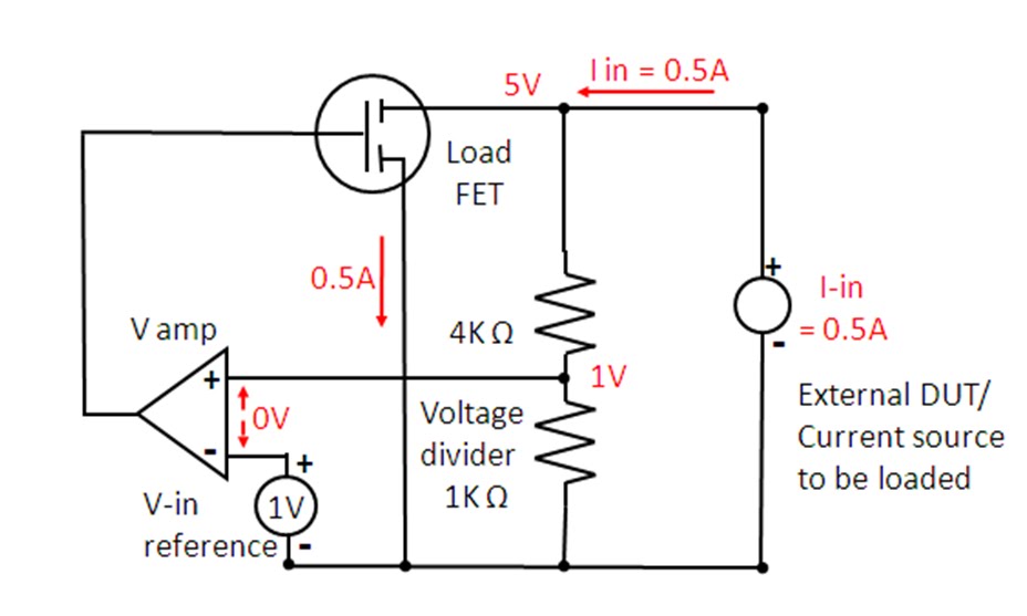
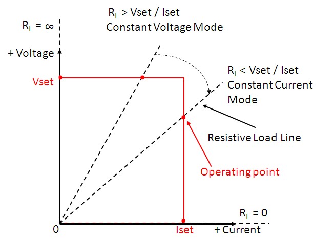
Most electronic loads provide constant current (CC), constant resistance (CR) and constant voltage (CV) loading. Some also offer constant power (CP) loading as well. The primary reason for this is this gives the test engineer a choice of loading that best addresses the loading requirement for the DUT, which invariably is some kind of power source.

Most usually the device should be tested with a load that reflects what the loading is like for its end use. In the most common case of a device being predominantly a voltage source the most common loading choices are either CC or CR loading, which we will look at in more detail here. Some feel they can be used interchangeably when testing a voltage source. To some extent this is true but in some cases only one or the other should be used as they can impact the DUT’s performance quite differently.

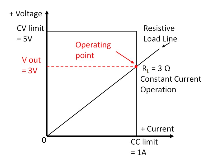
Let’s first consider static performance. In Figure 1 we have the output characteristics of an ideal voltage source with zero output resistance (a regulated power supply, for example) and a non-ideal voltage source having series output resistance (a battery, for example).  Both have the same open circuit (no load) voltage. Superimposed on these two source output characteristics are two load lines; one for CC and one for CR. As can be seen they are set to draw the same amount of current for the ideal voltage source. However, for the non-ideal voltage source, while the CC load still continues to draw the same amount of current in spite of the voltage drop, not surprisingly the CR load draws less current due to its voltage-dependent nature.


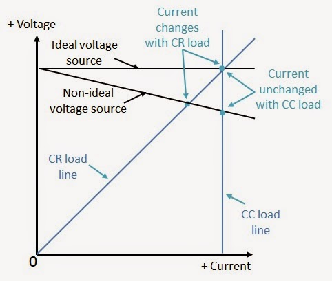
Figure 1: CC and CR loading of ideal and non-ideal voltage sources

CC loading is frequently used for static power supply tests for a key reason. Power supplies are usually specified to have certain output voltage accuracy for a fixed level of current. Using CC loading assures the loading condition is met, regardless of power supply’s output voltage being low or high, or in or out of spec. Non-ideal voltage sources, like batteries, present a little more of a problem and are often specified for both CC and CR loading as a result, to reflect the nature of the loading they may be subjected to in their end use. Due to a battery's load-dependent output voltage, trying to use one type of loading in place the other becomes an iterative process of checking and adjusting loading until the acceptable operating point is established.

Let’s now consider dynamic performance.  CC loading generally has a greater impact on a power supply’s ability to turn on as well as its transient performance and stability, in comparison to CR loading. When the power supply first starts up its output voltage is at zero. A CR load would demand zero current at start up. In comparison a CC load still demands full current. Some power supplies will not start up properly under CC loading. With regard to transient response and stability, CR loading provides a damping action, increasing current demand when the transient voltage increases and decreases demand when the transient voltage decreases, because the current demand is voltage dependent. CC loading does not do this, which can negatively influence transient response and stability somewhat. Whether CC or CR loading is used depends on what the power supply’s specifications call out for the test conditions. Batteries have some dynamic considerations as well. Their output response can be modeled as a series of time constants spanning a wide range of time. This presents somewhat of a moving target for an algorithm that uses an iterative approach to settling on an acceptable operating point.


This is just a couple of examples of how a load’s characteristic affects the performance of the device it is loading, and why electronic loads have multiple operating modes to select from, and worth giving thought next time towards how your device is affected by its loading!

Thursday, February 20, 2014

How to test the efficiency of DC to DC converters, part 1 of 2

I periodically get asked to provide recommendations and guidance on testing the efficiency of small DC to DC voltage converters. Regardless of the size of the converter, a DC source is needed to provide input power to the converter under constant voltage, while an electronic load is needed to draw power from the output, usually under constant current loading. The load current needs to be swept from zero to the full load current capability of the DC to DC converter while input power (input voltage times input current) and output power (output voltage times output current) are recorded. The efficiency is then the ratio of power out to power in, most often expressed in a percentage. An illustration of this is shown in Figure 1. In addition to sourcing and sinking power, precision current and voltage measurement on both the input and output, synchronized to the sweeping of the load current is needed.


Figure 1: DC to DC converter efficiency test set up

One challenge for small DC to DC voltage converters is finding a suitable electronic load that will operate at the low output voltages and down to zero load currents, needed for testing their efficiency over their range, from no load to full load output power. It turns out in practice many source measure units (SMUs) will serve well as a DC electronic load for testing, as they will sink current as well as source current.

Perhaps the most optimum choice from us is to use two of our N6782A 2-quadrant SMU modules installed in our N6705B DC Power Analyzer mainframe, using the 14585A software to control the set up and display the results.  This is a rather flexible platform intended for a variety of whatever application one can come up with for the most part. With a little ingenuity it can be quickly configured to perform an efficiency test of small DC to DC converters, swept from no load to full load operation. This is good for converters of 20 watts of power or less and within a certain range of voltage, as the N6782A can source or sink up to 6 V and 3 A or 20 V and 1 A, depending on which range it is set to. One of the N6782A operates as a DC voltage source to power the DUT and the second is operated as a DC current load to draw power from the DUT. A nice thing about the N6782A is it provides excellent performance operated either as a DC source or load, and operated either in constant voltage or constant current.

An excellent video of this set up testing a DC to DC converter was created by a colleague here, which you can review by clicking on the following link: “DC to DC converter efficiency test”.

The video does an excellent job covering a lot of the details. However, if you are interested in testing DC to DC converters using this set up I have a few more details to share here about it which should help you further along with setting it up and running it.

First, the two N6782A SMUs were set up for initial operating conditions. The N6782A providing DC power in was set up as a voltage source at the desired input voltage level and the second N6782A was set to constant current load operation with minimum (near zero) loading current.

Note that the 14585A software does not directly sweep the load current along the horizontal axis. The horizontal axis is time. That is why a time-based current sweep was created in the arbitrary waveform (ARB) section of the 14585A. In that way any point on the horizontal time axis correlates to a certain current load level being drawn from the output of the DUT. The ARB of course was set to run once, not repetitively. The 14585A ARB set up is shown in Figure 2.


Figure 2: Load current sweep ARB set up in 14585A software

This ARB sweep requires a little explanation.  While there are a number of pre-defined ARBs, and they can be used, an x3 power formula was chosen to be used instead. This provided a gradually increasing load sweep that allowed greater resolution of this data and display at light loads, where efficiency more quickly changes. As can be seen, the duration of the sweep, parameter x, was set to 10 seconds. As a full load current needed to be -1 A, using the actual formula (-x/10)3  gave us a gradually increasing load current sweep that topped out at -1A after 10 seconds of duration. The choice of 10 seconds was arbitrary. It only provided an easy way to watch the sweep on the 14585A graphing as it progressed. Finally, a short (0.1 second) pre-defined linear ramp ARB was added as a second part of the ARB sequence, to bring the load current back to initial, near zero, load conditions after the sweep was completed. This is shown in Figure 3.


Figure 3: Second part of ARB sweep to bring DUT load current back to initial conditions


I hope this gives you a number of insights about creative ways you can make use of the ARB. As there is a good amount of subtle details on how to go about making and displaying the measurements I’ll be sharing that in a second part coming up shortly, so keep on the outlook!

Wednesday, November 6, 2013

Paralleling power supplies for more power without compromising performance!

A year ago my colleague here, Gary, provided a posting “How can I get more power from my power supplies?” (Click here to review). He describes connecting power supplies in series for higher voltage or in parallel for higher current. Along with suggested set ups a list of requirements and precautions are also provided.

Connecting multiple power supplies in parallel operating as voltage sources is always problematic as there will be some imbalance of voltage between them. That’s why, in this previous posting, one unit operates as a voltage source and the remaining paralleled units operate in constant current. The compliance voltage limit of all the units operating in constant current need to be set higher than the master in operating in constant voltage in order to maintain this operation. This is illustrated in Figure 1.


Figure 1: Operating power supplies in parallel for higher power


As long as a high level of loading is maintained the paralleled units remain in their respective operating modes (in this case at least 2/3 loading). However, what happens if you cannot maintain that high level of loading? It is possible in practice to operate at lighter loads with this approach. In this case it is important to set the voltage levels of all the units the same. Now what happens is when the units are fully loaded they operate as already described, with the lowest voltage unit remaining in constant voltage. But when they are unloaded the lower voltage units transition to unregulated operation and the highest voltage unit then maintains the overall output in constant voltage. This is shown in Figure 2, for 0 to 1/3 loading.


Figure 2: Conditions of power supplies connected in parallel at light loading

There is a bit of performance compromises as a result. The transition between the lowest and highest voltage limits adds to the voltage regulation. Also, due to different units experiencing mode crossover transitions between constant voltage, constant current and unregulated operating modes transient voltage performance suffers considerably.

An improvement on this direct paralleling approach is having a master-slave arrangement with control signals to maintain current sharing across units. Our N5700A and N8700A series power supplies use such a control arrangement as depicted in Figure 3, taken from the N5700A user’s guide.


Figure 3: N5700A Connection for parallel operation (local sensing used)

With this arrangement the master unit, operating in constant voltage, provides an analog current programming output signal to the slave unit, operating in constant current. In this way the two units equally share the load current across a wide range of load current.

Still, having multiple units with only one in constant voltage does not provide as good of dynamic performance as a single voltage source of higher power.  A unique and innovative approach was taken with our N6900A / N7900A series Advance Power System (APS) to support seamless parallel operation without compromising performance. The paralleling arrangement for our N6900A / N7900A series APS is depicted in Figure 4.


Figure 4: N6900A / N7900A series APS Connection for parallel operation

The N6900A / N7900A series APS paralleling arrangement also uses an analog control signal for driving current sharing. However with this arrangement there is no master or slaves. All units remain in constant voltage while equally sharing current. This provides the user with an easy way to scale a power system as required without having to worry about compromising performance.

Monday, June 10, 2013

DC power supply output impedance characteristics

In a previous posting; “How Does a Power Supply regulate It’s Output Voltage and Current?” I showed how feedback loops are used to control a DC power supply’s output voltage and current.  Feedback is phenomenally helpful in providing a DC power supply with near-ideal performance. It is the reason why load regulation is measured in 100ths of a percent. A major reason for this is it bestows the power supply, if a voltage source, with near zero impedance, or as a current source, with high output impedance. How does it do this?

The impedance of a typical DC power supply’s output stage (like the conceptual one illustrated in the above referenced posting) is usually on the order of an ohm to a couple of ohms. This is the open-loop output impedance; i.e. the output impedance before any feedback is applied around the output.   If no feedback were applied we would not have anywhere near the load regulation we actually get. However, when the control amplifier provides negative feedback to correct for changes in output when a load is applied, the performance is transformed by the ratio of 1 + T, where T is loop gain of the feedback system. As an example, the output impedance of the DC power supply operating in constant voltage becomes:

Zout (closed loop) = Zout (open loop) / (1+T)

The loop gain T is approximately the gain of the operational amplifier times the attenuation of the voltage divider network. In practical feedback control systems the gain of the amplifier is quite large at and near DC, possibly as high as 90 dB of gain. This reduces the power supply’s DC and low frequency output to just milliohms or less, providing near ideal load regulation performance. Another factor in practical feedback control systems is the loop gain is rolled off in a controlled manner with increasing frequency in order to maintain stability. Thus at higher frequency the output impedance of a DC power supply operating as a voltage source increases towards its open loop impedance value as the loop gain decreases. This is illustrated in the output impedance plots in Figure 1, for the Agilent 6643A DC power supply.


Figure 1: Agilent 6643A 35V, 6A system DC power supply output impedance

As can be seen in Figure 1, for constant voltage operation, the 6643A DC power supply is just about 1 milliohm at 100 Hz, and exhibits an inductive output characteristic with increasing frequency as the loop gain decreases.

As also can be seen in Figure 1, feedback control works in a similar fashion for constant current operation. While a voltage source ideally has zero output impedance, a current source ideally has infinite impedance.  For constant current operation the 6643A DC power supply exhibits 10 ohms impedance at 100 Hz and rolls off in a capacitive fashion as frequency increases. However, for the 6643A, it is not so much the constant current control loop gain dropping off with frequency but the output filter capacitance dominating the output impedance. While the 6643A can be used as an excellent, well-regulated current source (see posting: “Can a standard DC power supply be used as current source?”) it is first and foremost optimized for being a voltage source. Some output capacitance serves towards that end.


An example of one use for the output impedance plots of a DC power supply is to estimate what the amount of load-induced AC ripple might be, based on the frequency and amplitude of the current being drawn by the load, when powered by power supply operating in constant voltage.

Tuesday, March 12, 2013

What is a power supply’s over current protect (OCP) and how does it work?


One feature we include in our Agilent system DC power supplies for providing additional safeguard for overload-sensitive DUTs is over current protect, or OCP. While some may think this is something separate and independent of current limiting, OCP actually works in concert with current limiting.

Current limiting protects overload-sensitive DUTs by limiting the maximum current that can be drawn by the DUT to a safe level. There are actually a variety of current limit schemes, depending on the level of protection required to safeguard the DUT during overload. Often the current limit is relatively constant, but sometimes it is not, depending on what is best suited for the particular DUT. Additional insights on current limits are provided in an earlier posting, entitled “Types of current limits for over-current protection on DC power supplies“.

By limiting the current to a set level may DUTs are adequately protect from too much current and potential damage. When in current limit, if the overload goes away the power supply automatically goes back to constant voltage (CV) operation. However, current limit may not be quite enough for some DUTs that are very sensitive to overloads. This is where OCP works together with the current limit to provide an additional level of protection. With OCP turned on, when the DC power supply enters into current limit OCP takes over after a specified time delay and shuts down the output of the DC power supply. The delay time is programmable. This prevents OCP from shutting down the DC power supply from short current spikes and other acceptably short overloads that are not considered harmful. Like over voltage protect or OVP, after tripping the output needs to be disabled and an Output Protect Clear needs to be exercised in order to reset the power supply so that its output can be re-enabled.  Unlike OVP, OCP can be turned on and off and its default is usually off. In comparison, OVP is usually always enabled and cannot be turned off. A typical OCP event is illustrated in Figure 1.


Figure 1: OCP operation

When powering DUTs, either on the bench or in a production test system, it is always imperative that adequate safeguards are taken to protect both the DUT as well as the test equipment from inadvertent damage. Over current protect or OCP is yet another of many features incorporated in system DC power supplies you can take advantage of to protect overload-sensitive DUTs from damage during test!

Friday, January 18, 2013

Types of current limits for over-current protection on DC power supplies


On a previous posting “The difference between constant current and current limit in DC power supplies”, I discussed what differentiates a DC power supply having a constant current operation in comparison to having strictly a current limit for over-current protection. In that post I had depicted one very conventional current limit behavior. However there is actually quite a variety of current limits incorporated in different DC power supplies, depending on the intended end-use of the power supply.

Fold-back Current Limit
The output characteristic of a constant voltage (CV) power supply utilizing fold-back current limiting is depicted in Figure 1. Fold-back current limiting is sometimes used to provide a higher level of protection for DUTs where excess current and power dissipation can cause damage to a DUT that has gone into an overload condition. This is accomplished by reducing both the current and voltage as the DUT goes further into overload. The short circuit current will typically be 20% to 50% of the maximum current level. A reasonable margin between the crossover current point and required maximum rated DUT current needs to be established in order to prevent false over-current tripping conditions. Due to the fold-back nature, and depending on the loading nature of the DUT, the operating point could drop down towards the short-circuit operating point once the crossover point is reached/exceeded. This would require powering the DUT down and up again in order to get back to the CV operating region.


Figure 1: Output characteristic of a CV power supply with fold-back current limiting

In addition to providing over-current protection for the DUT, fold-back current limiting is often employed in fixed output linear DC power supplies as a means for reducing worst case dissipation in the power supply itself. Under short circuit conditions the voltage normally appearing across the DUT instead appears across the power supply’s internal series linear regulator, requiring it to dissipate considerably more power than it has to under normal operating conditions. By employing fold-back current limiting the power dissipation on the series-linear regulator is greatly reduced under overload conditions, reducing the size and cost of the series-linear regulator for a given output power rating of the DC linear power supply.


Fold-forward Current Limit
A variety of loading devices, such as electric motors, DC-DC converters, and large capacitive loads can draw large peak currents at startup. Because of this they can often be better suited for being powered by a DC power supply that has a fold-forward current limit characteristic, as depicted in Figure 2. With fold-forward current limiting after exceeding the crossover current limit the current level instead continues to increase while the voltage drops while the loading increases.


Figure 2: Output characteristic of a CV power supply with fold-forward current limiting

As one example of where fold-forward current limiting is a benefit, it can help a motor start under load which otherwise would not start under other current-limits. Indeed, with fold-back current limiting, a motor may not and then it would remain stalled, due to the reduced current.

Special Purpose Current Limits
Unlike the previous current limit schemes which are widely standard practice, there is a number of other current limit circuits used, often tailored for more application-specific purposes. One example of this is the current limiting employed in our 66300 series DC sources for powering mobile phones and other battery powered mobile wireless devices. Its output characteristic is depicted in Figure 3.


Figure 3: Agilent 66300 Series DC source output characteristics

We refer to this power supply series as battery emulator DC sources. One reason why is they are 2-quadrant DC sources.  Like a rechargeable battery, they need to be able to source current when powering the mobile device and then sink current when the mobile device is in its charging mode.  In Figure 3 there are actually two separate current limits; one for sourcing current and another for sinking current. Each has different and distinctive characteristics for specific purposes.

Many battery powered mobile wireless devices draw power and current in short, high peak bursts, especially when transmitting. To better accommodate these short, high peaks, the 66300 series DC sources have a time-limited peak current limit that is of sufficient duration to support these high peaks. They also have a programmable constant current level that will over-ride the peak current limit when the average current value of the pulsed current drain reaches this programmed level. With this approach a higher peak power mobile device can be powered from a smaller DC power source.

Just like an electronic load, when the 66300 series DC source is sinking current the limiting factor is how much power it is able to dissipate. Instead of using a fixed current limit, it uses a fold-forward characteristic current limit (although folding forward in the negative direction!). This is not done for reasons that a fold-forward current limit that was just discussed is used; it is done so higher charging currents at lower voltage levels can be accommodated, taking advantage of the available power that can be dissipated. Again, this provides the user with greater capability in comparison to using a fixed-value limit.

Other types of current limits exist for other specific reasons so it is helpful to be aware that not all current limits are the same when selecting a DC power supply for a particular application!

Reference: Agilent Technologies DC Power Supply Handbook, application note AN-90B, part number 5952-4020 “Click here to access”

Tuesday, January 8, 2013

The difference between constant current and current limit in DC power supplies


Constant Voltage/Constant Current (CC/CV) Power Supplies
In most of our discussions in “Watt’s Up?” on current limiting we have primarily talked about power supplies as having a constant current (CC) output characteristic. This is what is found in many lab and industrial system power supplies, including most of the power supplies provided by us. Even though the terms often get used interchangeably, there is actually a distinction between constant current and current limit. To help explain this distinction, Figure 1 illustrates the output characteristics of a constant voltage/constant current (CV/CC) power supply.


Figure 1: Operating locus of a CC/CV power supply

Five operating points are depicted in Figure 1:
  1. With no load (i.e. infinite load resistance): Iout = 0 and Vout = Vset
  2. With a load resistance of RL > Vset/Iset: Iout = Vset/RL and Vout = Vset
  3. With a load resistance of RL = Vset/Iset: Iout = Iset and Vout = Vset
  4. With a load resistance of RL < Vset/Iset: Iout = Iset and Vout = Iset*RL
  5. With a short circuit (i.e. zero load resistance): Iout = Iset and Vout = 0


The advantage of a CV/CC power supply is it can be used as either a voltage source or a current source, providing reasonable performance in either mode. The point at which RL = Vset/Iset is the mode crossover point where the power supply transitions between CV and CC operation. For a CV/CC power supply there is a sharp transition between CV and CC operation. Note that for an ideal CV/CC power supply the CV slope is zero (horizontal), indicating zero output resistance for CV operation while the CC slope is infinite (vertical), indicating infinite output resistance for CC operation. Note that this is at DC. How close the slope of each mode is to ideal is what determines quality of load regulation for each.  To achieve good performance for both CV and CC modes requires carefully designed and more complex control loops for each mode. More details about using a power supply as a current source is provided in an earlier posting here, entitled: “Can a standard DC power supply be used as a current source?”

Constant Voltage/Current Limiting Power Supplies
In comparison a constant voltage/current limiting (CV/CL) power supplies are intended to be used only as a voltage source while providing over-current protection for the DUT, as well as protection for the power supply itself. Figure 2 depicts typical output characteristics of a CV/CL power supply.


Figure 2: Operating locus of a CV/CL power supply

In CV/CL power supplies the current limit may be a fixed maximum value or it may be settable. In comparison to Figure 1 CV operation is still the same. However, what is found at the current limit cross-over point there is loss of voltage regulation where the voltage starts falling off. Unlike true CC operation in a CV/CC power supply, CL operation does not typically have as sharply a defined cross-over point and once in CL it may not be tightly regulated between the cross-over and short circuit points. The reason for this is CL control circuits are usually more basic in nature in comparison to a true CC control loop. CL is meant for over-current protection only, not CC operation.  For this reason the correct use of CL is to set its value a bit higher than the maximum current required by the DUT. This assures good voltage regulation for the full range of normal loading. You may find many of the more basic bench power supplies have CV/CL operation and may not be useful as current sources as a result.

Reference: Agilent Technologies DC Power Supply Handbook, application note AN-90B, part number 5952-4020

Monday, December 10, 2012

More on power supply current source-to-sink crossover characteristics


On my earlier posting “Power supply current source-to-sink crossover characteristics” I showed what the effects on the output voltage of a unipolar two-quadrant-power supply were, resulting from the output current on the power supply transitioning between sourcing and sinking. In that example scenario, the power supply was maintaining a constant output voltage and the transitioning between sourcing and sinking current was dictated by the external device connected to and being powered by the power supply. This is perhaps the most common scenario one will encounter that will drive the power supply between sourcing current and sinking current.

Other scenarios do exist that will drive a unipolar two-quadrant power supply to transition between sourcing and sinking output current. One scenario is nearly identical to the earlier posting. However, instead of the device transitioning its voltage between being less and greater than the power supply powering it, the power supply instead transitions its voltage between being less and greater than the active device being normally powered.  A set up for evaluating this scenario on an Agilent N6781A two-quadrant DC source is depicted in Figure 1.


Figure 1: Evaluating current source-to-sink crossover on an N6781A operating in constant voltage

In this scenario having the DC source operating as a voltage source and transitioning between 1.5 and 4.5 volts causes the current to transition between -0.75 and +0.75A.  The voltage and current waveforms captured on an oscilloscope are shown in Figure 2.


Figure 2: Voltage and current waveforms for the set up in Figure 1

The waveforms in Figure 2 are as what should be expected. The actual transition points are where the current waveform passes through zero on the rising and falling edge. An expanded view to the current source-to-sink transition is shown in Figure 3.


Figure 3: Expanded voltage and current waveforms for the set up in Figure 1

As can be seen the voltage ramp transitions smoothly at the threshold point, or zero crossing point, of the current waveform. The reason being is that the DC is maintaining its operation as a voltage source. Its voltage feedback loop is always in control.


Yet one more scenario that will drive a unipolar two-quadrant source to transition between sourcing and sinking current is operate it as a current source and program is current setting between positive and negative values. In this case the device under test that was used is a voltage source.  One real-world example is cycling a rechargeable battery by alternately applying charging and discharging currents to it. The set up for evaluating this scenario, again using an N6781A two-quadrant DC source is depicted in Figure 4.


Figure 4: Evaluating current source-to-sink crossover on an N6781A operating in constant current

For Figure 4 the N6781A was set to operate in constant current and programmed to alternately transition between -0.75A and +0.75A current settings. The resulting voltage and current waveforms are shown in Figure 5.


Figure 5: Voltage and current waveforms for the set up in Figure 4

The waveforms in Figure 5 are as what should be expected. The actual transition points are where the current waveform passes through zero on the rising and falling edge. An expanded view to the current source-to-sink transition is shown in Figure 6.


Figure 6: Expanded voltage and current waveforms for the set up in Figure 4

As the N6781A is operating in current priority the interest is in how well it controls its current while transitioning through the zero-crossing point. As observed in Figure 6 it transitions smoothly through the zero-crossing point. The voltage performance is determined by the DUT, not the N6781A, as the N6781A is operating in constant current.

So what was found here is, for a unipolar two-quadrant DC source, transitioning between sourcing and sinking current should generally be virtually seamless as, under normal circumstances, should remain in either constant voltage or constant current during the entire transition.

Wednesday, December 5, 2012

Power supply current source-to-sink crossover characteristics


A two-quadrant power supply is traditionally one that outputs unipolar voltage but is able to both source as well as sink current. For a positive polarity power source, when sourcing current it is operating in quadrant 1 as a conventional power source. When sinking current it is operating in quadrant 2 as an electronic load. Conversely, a negative polarity two-quadrant  power source operates in quadrants three and four. Further details on power supply operating quadrants are provided in a recent posting here in ‘Watt’s Up?”, What is a bipolar (four-quadrant) power supply? Often a number of questions come up when explaining two-quadrant power supply operation, including:
  • What does it take to get the power supply operating as a voltage source to cross over from sourcing to sinking current?
  • What effect does crossing over from sourcing to sinking current have on the power supply’s output?


For a two-quadrant voltage source to be able to operate in the second quadrant as an electronic load, the device it is normally powering must also be able to source current and power as well as normally draw current and power. Such an arrangement is depicted in Figure 1, where the device is normally a load, represented by a resistance, but also has a charging circuit, represented by a switch and a voltage source with current-limiting series resistance.


Figure 1: Voltage source and example load device arrangement for two-quadrant operation.

There is no particular control on a two-quadrant power supply that one has to change to get it to transition from sourcing current and power to sinking current and power from the device it is normally powering. It is simply when the source voltage is greater than the device’s voltage then the voltage source will be operating in quadrant one sourcing power and when the source voltage is less than the device’s voltage the voltage source will be operating in quadrant two as an electronic load. In figure 1, during charging the load device can source current back out of its input power terminals as long as the charger’s current-limited voltage is greater than the source voltage.

It is assumed that load device’s load and charge currents are lower than the positive and negative current limits of the voltage source so that the voltage source always remains in constant voltage (CV) operation. A step change in current is the most demanding from a transient standpoint, but as the voltage source is always in its constant voltage mode it handle the transition well as its voltage control amplifier is always in control. This is in stark contrast to a mode cross over between voltage and current where different control amplifiers need to exchange control of the power supply’s output. In this later case there can be a large transient while changing modes. See another posting, Why Does My Power Supply Overshoot at Current Limit? Insights on Mode Crossover” for further information on this.  There is a specification given on voltage sources which quantifies the impact one should expect to see from a step change in current going from sourcing current to sinking current, which is its transient voltage response.  A transient voltage response measurement was taken on an N6781A two-quadrant DC source, stepping the load from 0.1 amps to 1.5 amps, roughly 50% of its rated output current.


Figure 2: Agilent N6781A transient voltage response measurement for 0.1A to 1.5A load step

However, the transient voltage response shown in Figure 2 was just for sourcing current. With a well-designed two-quadrant voltage source the transient voltage response should be virtually unchanged for any step change in current load, as long as it falls within the voltage source’s current range.  The transient voltage response for an N6781A was again capture in Figure 3, but now for stepping the load between -0.7A and +0.7A.


Figure 3: Agilent N6781A transient voltage response measurement for -0.7A to +0.7A load step

As can be seen in Figures 2 and 3 the voltage transient response for the N6781A remained unchanged regardless of whether the stepped load current was all positive or swung between positive and negative (sourcing and sinking).

While the transient voltage response addresses the dynamic current loading on the voltage source there is another specification that addresses the static current loading characteristic, which is the DC load regulation or load effect.  This is a very small effect on the order of 0.01% output change for many voltage sources. For example, for the N6781A the load effect in its 6 volt range is 400 microvolts for any load change. In the case of the N6781A being tested here the DC change was the same for both the 0.1 to 1.5 amp step and the -0.7 to +0.7 amp step change.


There are two more scenarios which will cause a two-quadrant power supply transition between current sourcing and sinking.  The first is very similar to above with the two-quadrant power supply operating in constant voltage (CV) mode, but instead of the DUT changing, the power supply changes its voltage level instead.  The final scenario is having the two-quadrant power supply operating in constant current with the DUT being a suitable voltage source that is able to source and sink power as well, like a battery for example. Here the two-quadrant power supply can be programmed to change from a positive current setting to a negative current setting, thus transitioning between sourcing and sinking current again, and its current regulating performance is now a consideration.  Both good topics for future postings!

Tuesday, August 7, 2012

How Does an Electronic Load Regulate It’s Input Voltage, Current, and Resistance?


In a sense electronic loads are the antithesis of power supplies, i.e. they sink or absorb power while power supplies source power. In another sense they are very similar in the way they regulate constant voltage (CV) or constant current (CC). When used to load a DUT, which inevitably is some form of power source, conventional practice is to use CC loading for devices that are by nature voltage sources and conversely use CV loading for devices that are by nature current sources. However most all electronic loads also feature constant resistance (CR) operation as well. Many real-world loads are resistive by nature and hence it is often useful to test power sources meant to drive such devices with an electronic load operating in CR mode.

To understand how CC and CV modes work in an electronic load it is useful to first review a previous posting I wrote here, entitled “How Does a Power Supply Regulate It’s Output Voltage and Current?”. Again, the CC and CV modes are very similar in operation for both a power supply and an electronic load. An electronic load CC mode operation is depicted in Figure 1.


Figure 1: Electronic load circuit, constant current (CC) operation

The load, operating in CC mode, is loading the output of an external voltage source. The current amplifier is regulating the electronic load’s input current by comparing the voltage on the current shunt against a reference voltage, which in turn is regulating how hard to turn on the load FET. The corresponding I-V diagram for this CC mode operation is shown in Figure 2. The operating point is where the output voltage characteristic of the DUT voltage source characteristic intersects the input constant current load line of the electronic load.


Figure 2: Electronic load I-V diagram, constant current (CC) operation

CV mode is very similar to CC mode operation, as depicted in Figure 3.  However, instead of monitoring the input current with a shunt voltage, a voltage control amplifier compares the load’s input voltage, usually through a voltage divider, against a reference voltage. When the input voltage signal reaches the reference voltage value the voltage amplifier turns the load FET on as much as needed to clamp the voltage to the set level.


Figure 3: Electronic load circuit, constant voltage (CV) operation

A battery being charged is a real-world example of a CV load, charged typically by a constant current source. The corresponding I-V diagram for CV mode operation is depicted in figure 4.


Figure 4: Electronic load I-V diagram, constant voltage (CV) operation

But how does an electronic load’s CR mode work? This requires yet another configuration, as depicted in figure 5. While CC and CV modes compare current and voltage against a reference value, in CR mode the control amplifier compares the input voltage against the input current so that one is the ratio of the other, now regulating the input at a constant resistance value.  With current sensing at 1 V/A and voltage sensing at 0.2 V/V, the electronic load’s resulting  input resistance value is 5 ohms for its CR mode operation in Figure 5.


Figure 5: Electronic load circuit, constant resistance (CR) operation

An electronic load’s CR mode is well suited for loading a power source that is either a voltage or current source by nature. The corresponding I-V diagram for this CR mode for loading a voltage source is shown in Figure 6. Here the operating point is where the output voltage characteristic of the DUT voltage source intersects the input constant resistance characteristic of the load.


Figure 6: Electronic load I-V diagram, constant resistance (CR) operation

As we have seen here an electronic load is very similar in operation to a power supply in the way it regulates to maintain constant voltage or constant current at its input.  However many real-world loads exhibit other characteristics, with resistive being most prevalent. As a result most all electronic loads are alternately able to regulate their input to maintain a constant resistance value, in addition to constant voltage and constant current.

Monday, July 23, 2012

Why Does My Power Supply Overshoot at Current Limit? Insights on Mode Crossover


One often encountered issue with power supply use is expecting that the current limit will clamp the current to no greater than the set value, only to discover the current initially overshoots when the DUT demands current in excess of the set limit. In some cases the short surge of excess current may be enough to damage a sensitive DUT. Those experienced with power supplies will recognize this as a dynamic characteristic of mode crossover.

What is mode crossover? Mode crossover is the transition point between Constant Voltage (CV) and Constant Current (CC) modes. The dynamic response characteristic of mode crossover is an aspect that separates real-world from ideal-world power supplies. To start it will be helpful to review a previous posting on “How Does a Power Supply regulate its Output Voltage and Current?” Here it is shown there are two control loops in most power supplies, one for regulating the voltage and one for regulating the current. Only one is in control at any given time while the other is “open loop”. The error amplifier that is open loop is up against it stops. When load conditions change such that the power supply transitions through mode crossover the open loop error amplifier needs to recover and gain control of the output. In the more common case of the power supply operating as a voltage source there can be a current overshoot during the brief moment when the load increases beyond the power supply’s current limit setting. Conversely, for a current source, there can be a voltage overshoot during the brief moment when the load decreases, causing the output voltage to rise to the voltage limit setting.

The magnitude of the overshoot depends on many factors relating to both the power supply and the DUT. Supplementary circuitry usually surrounds the error amplifiers to clamp them from being driven into saturation or cutoff so that they can more quickly recover when needed. Amplifiers are carefully selected for their recovery characteristics. Careful design is required to assure a stable transition between modes during crossover while at the same time minimizing the delay and overshoot.  The magnitude of the overshoot also depends on how quickly and to what extent the DUT transitions between loading conditions.

Figure 1 shows the mode crossover current overshoot of a 50 volt, 3 amp general purpose power supply, set for 10 volts and 1 amp output.  The loading DUT is an electronic load set to transition from no load to 10 amps with a slew of 0.8 amps per microsecond. This loading represented a worst case for all practical purposes. When the load transitions to full (i.e. overload) it takes about 6 milliseconds for the current limit control loop to fully take over and bring the current down. During this mode crossover period the current overshoot plateaus at 5 amps, which is the gross current limit capacity of the power supply. Basically this is the point where the power supply runs out of drive.


Figure 1: Constant voltage to constant current mode crossover for 10 V, 1A power supply settings

In Figure 2 the power supply current limit was reduced to 0.1 amps and the mode crossover was again captured. This had an interesting impact on the current overshoot. While the peak current still hit a plateau of 5 amps, the duration of the overshoot was considerably reduced to about 0.5 milliseconds.  The reason for this is there was a much larger difference driving the error amplifier’s input, causing it to transition more quickly. The peak level remained unchanged as it is determined by the power supply’s gross current limit capacity, which is fixed.


Figure 2: Constant voltage to constant current mode crossover for 10 V, 0.1A power supply settings

The extent of an overshoot during mode crossover depends on the power supply as well as the DUT. A power supply optimized for voltage sourcing usually has very little voltage overshoot at mode crossover, but then can have significant current overshoot, as we see here. Conversely, a power supply optimized for current sourcing usually has very little current overshoot at mode crossover, but then can have significant voltage overshoot. Higher performance power supplies may provide faster and better mode crossover performance, but this usually comes at greater expense. Some useful things to do include:
·         Be aware that overshoot during mode crossover is a reality that exists in most all power supplies
·         Try not to oversize the power supply. Be aware that the peak level of voltage or current during mode crossover may be governed more by the maximum voltage and current ratings of the power supply and less by the settings. Using an oversized power supply with its limit set to 5% of its capacity will likely yield a much larger overshoot than a smaller one with it limit set to 50% of its capacity.
·         Understand the nature of your DUT, behavior or fault modes that may cause it to draw an overload, and how sensitive it is to an overload
·         If your DUT is sensitive to an overload, include evaluating the response characteristics of mode crossover as part of your evaluation, using realistic conditions that reflect the characteristics of your DUT.

Recognizing that there is dynamic response characteristics associated with mode crossover of “real-world” power supplies, and they need to be considered, may save a lot of surprise and frustration later on!

Tuesday, July 17, 2012

How Does a Power Supply regulate It’s Output Voltage and Current?


We have talked about Constant Voltage (CV) and Constant Current (CC) power supply operation in many various ways and applications here on the “Watt’s Up?” blog in the past. Indeed, CV and CC are fundamental operating modes of most all power supplies. But what exactly takes place inside the power supply that endows it with the ability to regulate either its output voltage or current, depending on the load? If you ever wondered about this, wonder no longer!

Most all power supplies regulate either their output voltage or output current at a constant level, depending on the load resistance relative to the power supply’s output voltage and current settings. This can be summarized as follows:

·         If R load > (V out / I out) then power supply is in CV mode
·         If R load < (V out / I out) then power supply is in CC mode

To accomplish this most all power supplies have separate voltage and current feedback control loops to limit either the output voltage or current, depending on the load. To illustrate this Figure 1 shows a circuit diagram of a basic 5 volt, 1 amp output series regulated power supply operating in CV mode.


Figure 1: Basic DC Power Supply Circuit, Constant Voltage (CV) Operation

The CV and CC control loops/amplifiers each have a reference input value. In this case the reference values are both 1 volt. In order to regulate output voltage the CV error amplifier compares its 1 volt reference against a resistor divider that divides the output voltage down by a factor of 5, limiting the output voltage to 5 volts. Likewise the CC error amplifier compares its 1 volt reference against a 1 ohm current shunt resistor located in the output current path, limiting the output current to 1 amp. For Figure 1 the load resistance is 10 ohms. Because this load resistance is greater than (V out / I out) = 5 ohms, the power supply is operating in CV mode. The CV error amplifier takes control of the series pass transistor by drawing away excess base current from the series pass transistor, though the diode “OR” network. The CV amplifier is operating in closed loop, maintaining its error voltage at zero volts. In comparison, because the actual output current is only 0.5 amps the CC amplifier tries to turn the current on harder but cannot because the CV amplifier has control of the output. The CC amplifier is operating open loop. Its output goes up to its positive limit while it has -0.5 volts of error voltage. The output I-V diagram for this Constant Voltage operation is shown in Figure 2.


Figure 2: Power Supply I-V Diagram, CV Operation

Now say we increase the load by lowering the output load resistance from 10 ohms down to 3 ohms. Figure 3 shows the circuit diagram of our basic 5 volt, 1 amp output series regulated power supply revised for operating in CC mode with a 3 ohm load resistor.


Figure 3: Basic DC Power Supply Circuit, Constant Current (CC) Operation

Because the load resistor is lower than (V out / I out) = 5 ohms, the power supply switches to CC mode. The CC error amplifier takes control when the voltage drop on the current shunt resistor increases to match the 1 volt reference value, corresponding to 1 amp output, drawing excess base current from the series pass transistor though the diode “OR” network. The CC amplifier is now operating closed loop, regulating the output current to maintain its input error voltage at zero. In comparison, because the actual output voltage is now only 3 volts the CV amplifier tries to increase the output voltage but cannot because the CC amplifier has control of the output. The CV amplifier is operating open loop. Its output now goes up to its positive limit while it has -0.4 volts of error voltage. The output I-V diagram for this Constant Current operation is shown in Figure 4.


Figure 4: Power Supply I-V Diagram, CC Operation

As we have seen most all power supplies have separate current and voltage control loops to regulate their outputs in either a Constant Voltage (CV) or in a Constant Current (CC) mode. One or the other takes control, depending on that the load resistance is in relation to what the power supply’s output voltage and current settings are. In this way both the load and power supply are protected by limiting the voltage and current that is delivered by the power supply to the load. By understanding this theory behind a power supply’s CV and CC operation it is also easier to understand the underlying reason for why various power supply characteristics are the way they are, as well as see how other power supply capabilities can be created by building on top of this foundation. Stay tuned!

Wednesday, March 28, 2012

What Is Going On When My Power Supply Displays “UNR”?

Most everyone is familiar with the very traditional Constant Voltage (CV) and Constant Current (CC) operating modes incorporated in most any lab bench or system power supply. All but the most very basic power supplies provide display indicators or annunciators to indicate whether it is in CV or CC mode. However, moderately more sophisticated power supplies provide additional indicators or annunciators to provide increased insight and more information about their operating status. One annunciator you may encounter is seeing “UNR” flash on, either momentarily or continuously. It’s fairly obvious that this means that the power supply is unregulated; it is failing to maintain a Constant Voltage or Constant Current. But what is really going on when the power supply displays UNR and what things might cause this?
To gain better insight about CV, CC and UNR operating modes it is helpful to visualize what is going on with an IV graph of the power supply output in combination with the load line of the external device being powered. I wrote a two part post about voltage and current levels and limits which you may find useful to review. If you like you can access it from these links levels and limits part 1 and levels and limits part 2. This posting builds nicely on these earlier postings. A conventional single quadrant power supply IV graph with resistive load line is depicted in Figure 1. As the load resistance varies from infinity to zero the power supply’s output goes through the full range of CV mode through CC mode operation. With a passive load like a resistor you are unlikely to encounter UNREG mode, unless perhaps something goes wrong in the power supply itself.
Figure 1: Single quadrant power supply IV characteristic with a resistive load

However, with active load devices you have a pretty high chance of encountering UNR mode operation, depending where the actual voltage and current values end up at in comparison to the power supply’s voltage and current settings. One common application where UNR can be easily encountered is charging a battery (our external active load device) with a power supply. Two different scenarios are depicted in Figure 2. For scenario 1, when the battery voltage is less than the power supply’s output, the point where the power supply’s IV characteristic curve and the battery’s load line (a CV characteristic) intersect, the power supply is in CC mode, happily supplying a regulated charge current into the battery. However, for scenario 2 the battery’s voltage is greater than the power supply’s CV setting (for example, you have your automobile battery charger set to 6 volts when you connect it to a 12 volt battery). Providing the power supply is not able to sink current the battery forces the power supply’s output voltage up along the graph’s voltage axis to the battery’s voltage level. Operating along this whole range of voltage greater than the power supply’s output voltage setting puts the power supply into its UNR mode of operation.
Figure 2: Single quadrant power supply IV characteristic with a battery load

A danger here is more sophisticated power supplies usually incorporate Over Voltage Protection (OVP). One kind of OVP is a crowbar which is an SCR designed to short the output to quickly bring down the output voltage to protect the (possibly expensive) device being powered. When connected to a battery if an OVP crowbar is tripped, damage to the power supply or battery could occur due to batteries being able to deliver a fairly unlimited level of current. It is worth knowing what kind of OVP there is in a power supply before attempting to charge a battery with it. Better yet is to use a power supply or charger specifically designed to properly monitor and charge a given type of battery. The designers take these things into consideration so you don’t have to!
I have digressed here a little on yet another mode, OVP, but it’s all worth knowing when working with power supplies! Can you think of other scenarios that might drive a power supply into UNR? (Hint: How about the other end of the power supply IV characteristic, where it meets the horizontal current axis?)