Showing posts with label DC Power Supply. Show all posts

Monday, February 9, 2015

Consider using an electronic load for generating fast, high-power current pulses

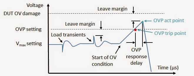
Often there is the need for generating high-power current pulses, typically of short duration, and having rise and fall times on the order of microseconds. This is a common need when testing many types of power semiconductors, for example.

When looking for a DC power supply capable of generating very fast, high-power current pulses, one will find there are not a lot of options readily available that are capable of addressing their needs. There are specialized products dedicated for specific applications like this; an example of this is Keysight’s B1505A purpose-built semiconductor test equipment. They are capable of generating extremely fast, high-power current pulses.

Apart from specialized products however, DC power supplies generally to not offer this kind of speed when operating in a constant current mode (or current priority mode). One exception that comes to mind that we provide is our N6782A and N6782A DC source measure modules. They can create fast current pulses having just a couple of microseconds of rise and fall time. However, they are limited to 20V, 3A, and 20W of output. Most of the higher power, more general-purpose DC sources are not able to generate these kinds of fast, high-power current pulses and most are really more optimized to operate as voltage sources.

One alternative to consider for generating fast, high-power current pulses when working with general-purpose test equipment is to use an electronic load. You may initially say to yourself “an electronic load is for drawing pulses of current, not sourcing them!” but when coupled to a standard DC power supply operating as a voltage source, the setup is able to source fast, high-power current pulses. Most electronic loads are designed to have very fast current response. To illustrate this, I helped one customer needing to test their high brightness LED (HBLED) arrays with fast pulses of current. This was accomplished with the setup shown in Figure 1.


Figure 1: Load setup generating fast, high power current pulses for LED array testing

In this setup the power supply operates as a fixed, static voltage source. The power supply’s output voltage is set to the combined total of the full voltage needed to drive the HBLED array at full current plus the minimum voltage needed for the electronic load. The minimum voltage required for the electronic load is when it conducting maximum current and most of the power supply voltage is then applied across the HBLED array. The electronic load’s required minimum voltage is that which supports its operation in its linear range and maintains full dynamic response characteristics. In the case of Keysight electronic loads this minimum voltage for linear dynamic operation is 3 volts.  Conversely the maximum voltage required for the electronic load is when it drops down to minimum current level, where the power supply’s voltage is instead now being dropped across the electronic load instead of the HBLED array. Note that the electronic load may need to maintain a very small amount of bleed current to maintain linear operation in order to provide truly fast rise and fall times. In this way the electronic load is able to regulate the current across the full 
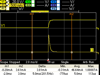
range with excellent dynamic response. This can be seen in Figure 2 where we were able to achieve approximately 15 microsecond rise time right from the start.


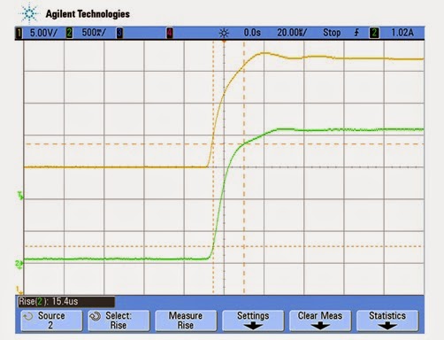
Figure 2: Pulsed current rise time in HBLED array

One advantage of this setup is the wide range of voltage and power that can be furnished to the DUT using a relatively low power electronic load. A common characteristic of electronic loads is that they can dissipate a given amount of power over an extended range of current and voltage. When the electronic load is at maximum current it is at minimum voltage. Conversely when it is near or at zero current it is then at its maximum voltage. In both cases there is only a small amount of power that the electronic load needs to dissipate. For an HBLED array it does not conduct a lot of current until it reaches about 75% of its full operating voltage. As a result the electronic load does not see a lot of power even on a transient basis. For this particular situation we chose to use the Keysight N3303A 240V, 10A, 250W electronic load. This gave a wide range of voltage, current, and power for testing a comparably wide range of different HBLED array assemblies.

So next time you need to source fast, high-power current pulses, you may want to think “load” instead of “source”!


Wednesday, December 31, 2014

Why is the Programming Resolution Supplemental Characteristic Listed as an Average?

Hello everyone!

Happy New Year!  This is our last post of 2014 so we wanted to wish all of our readers a Happy New Year.  Today I am going to talk about a question that I have been asked a few times lately.  In many of our power supplies, we list our Programming Resolution as an average number.  Many people want to know why we do it this way.

Look at the below snippet from our 664xA DC Power Supplies Supplemental Characteristics:


You can see that that it is clearly stated as an average.

The simple answer to this question is that this is because of calibration.

The more complex answer is that we use a DAC to control the output setting of the power supply.  A certain number of DAC counts is going to represent zero to full scale on the output of the supply.  For simplicity's sake, lets assume that we are using a 12 bit DAC for a power supply that goes to fifty volts.

In an ideal world where calibration is not necessary:
A 12 bit DAC gives us 2^12 or 4096 total counts.
The step size (programming resolution) of the 50 volt power supply would be 50/4096 or 0.0122 volts.

We do not live in an ideal world though so we have to disregard some DAC counts because of how the unit calibrates. We also generally let you program a little bit above the maximum settings (usually something like 2%).  Zero volts is not going to be zero DAC Counts and 50 V is not going to be 4096 DAC counts.  For our example, lets say that the minimum that we disregard 20 counts at the top and bottom (40 total counts) and the maximum we disregard is 120 counts (240 total counts) at the top and bottom.  In this scenario:

Minimum step size = 50/(4096-40) = 0.0123 V
Maximum step size = 50/(4096-120) = 0.0130 V

For our Supplemental Characteristic, we would take the average of those 2 numbers.   This gives us 0.01265 V.

The big question is how would I know what the programming resolution is for my particular unit.  I spent about half of yesterday trying to figure that out and I'm still working that out myself.  The best solution that I have right now is to hook a DMM to the output and slowly increment my output to see when it flips to a new setting.  I need to experiment on this though.  If any readers have a better idea, please let us know in the comments.  The fact of the matter is that the error is pretty small and to be safe, any error due to being in between DAC counts is included in our Programming Accuracy specification.

Well that is all for 2014. I hope that everyone has a safe and happy 2015.  See you next year!

Matt

Friday, November 7, 2014

Providing effective protection of your DUT against over voltage damage during test

The two most common ways DUTs can be electrically damaged during test are from current-related events or voltage-related events that mange to over-stress the DUT. Sometimes the cause can be an issue with the DUT itself. Other times it can be an issue stemming from the test system. The most common voltage-related damage to a DUT is an over voltage event, beyond a maximum level the DUT can safely tolerate. While there are a number of things that can cause this, most invariably it was an issue with the test system power supply, either from inadvertently being set too high or from an internal failure.

To protect against accidental over voltage damage, test system power supplies incorporate an over voltage protect (OVP) system that quickly shuts down the output upon detecting the voltage has gone above a preset threshold value. More details about OVP have been written about here in a previous posting “Overvoltage protection: some background and history”(click here to review).

The critical thing about over voltage damage is, in most all cases, that it is virtually immediate once the voltage threshold where damage to the DUT occurs is exceeded. It is therefore imperative that you optimize the test set up and settings in order to provide effective protection of your DUT against over voltage damage during test. To start with, the OVP trip threshold needs to be set at a reasonable amount below the threshold where DUT damage occurs and at the same time be set to a reasonable amount above the maximum expected DUT operating voltage. This is depicted in Figure 1.


Figure 1: OVP set point

However, to understand what are “reasonable amounts” above the maximum operating voltage and below the DUT damage voltage levels you need to take into account the dynamic response characteristics of the power supply output and OVP system, as depicted in Figure 2.


Figure 2: Power supply output and OVP dynamic response characteristics

It is important to have adequate margin above the maximum operating voltage to account for transient voltages due to the DUT drawing current from the power supply and resulting voltage response of the power supply in correcting for this loading, in order to prevent false OVP tripping. It is likewise important to adequate margin below the DUT damage threshold as it takes a small amount of time, in the range of 10’s to 100’s of microseconds, for the OVP system to start shutting down the power supply’s output once the OVP trip point has been crossed. At the same time the power supply typically has a maximum rate the output voltage can slew in. In practice these “reasonable amounts” typically need to be a few tenths to several tenths of a volt as a minimum.

Generally these margins are not difficult to manage, except when the DUT’s operating voltage is very small or the DUT operating current is very large producing a correspondingly large voltage drop in the power supply wiring. This is because the OVP is traditionally sensed on power supply’s output power terminals, so that it provides protection regardless of what the status and condition of the remote voltage sense wiring connection is. To improve on this we also provide OVP sensing on the remote sensing wires as an alternative to, or in addition to, the traditional sensing on the output power terminals. More details about this are described in another posting here “Protect your DUT: Use sense leads for over voltage protection (OVP)”(click here to review).

By following these suggestions you should be able to effectively protect your DUT against over voltage damage during test as well!

Monday, April 28, 2014

Upcoming Seminar on Using Your Power Supply to Improve Test Throughput

I have provided here on “Watt’s up?” a number of ideas on how you can improve your test throughput from time to time, as it relates on how to make better use of you system power supplies to accomplish this. I have categorized these ideas on how to improve throughput as either fundamental or advanced.

In “How fundamental features of power supplies impact your test throughput” (click here to review) I shared in a two-part posting definitions of key fundamental power supply features that impact test throughput and ways to make improvements to literally shave seconds off of your test time.

One example (of several) of an advanced idea on improving throughput I previously shared here is “Using the power supply status system to improve test throughput” (click here to review). Here I explain how, by monitoring the status system, you can improve throughput by not relying on using excessively long fixed wait statements in your programming.

I hope you have found these ideas helpful. If you would like to learn more about using your system power supply to improve your test throughput I will be presenting a live web-based seminar this week, in just a couple of days, April 30th, at 1:00 PM EST on this very topic!

In this seminar I will go through a number of things I’ve shared here on “Watt’s up?” in the past, but in greater detail. In addition, I have also prepared several new ideas as well in this seminar that you might find of help for your particular test situation.  You can register online at the following (click here to access seminar description and registration).  In case you miss the live event I expect you will be able to register and listen to seminar afterward as well, as it will be recorded.

So if improving your test throughput is important to you I hope you are able to attend the seminar!


Thursday, February 20, 2014

How to test the efficiency of DC to DC converters, part 1 of 2

I periodically get asked to provide recommendations and guidance on testing the efficiency of small DC to DC voltage converters. Regardless of the size of the converter, a DC source is needed to provide input power to the converter under constant voltage, while an electronic load is needed to draw power from the output, usually under constant current loading. The load current needs to be swept from zero to the full load current capability of the DC to DC converter while input power (input voltage times input current) and output power (output voltage times output current) are recorded. The efficiency is then the ratio of power out to power in, most often expressed in a percentage. An illustration of this is shown in Figure 1. In addition to sourcing and sinking power, precision current and voltage measurement on both the input and output, synchronized to the sweeping of the load current is needed.


Figure 1: DC to DC converter efficiency test set up

One challenge for small DC to DC voltage converters is finding a suitable electronic load that will operate at the low output voltages and down to zero load currents, needed for testing their efficiency over their range, from no load to full load output power. It turns out in practice many source measure units (SMUs) will serve well as a DC electronic load for testing, as they will sink current as well as source current.

Perhaps the most optimum choice from us is to use two of our N6782A 2-quadrant SMU modules installed in our N6705B DC Power Analyzer mainframe, using the 14585A software to control the set up and display the results.  This is a rather flexible platform intended for a variety of whatever application one can come up with for the most part. With a little ingenuity it can be quickly configured to perform an efficiency test of small DC to DC converters, swept from no load to full load operation. This is good for converters of 20 watts of power or less and within a certain range of voltage, as the N6782A can source or sink up to 6 V and 3 A or 20 V and 1 A, depending on which range it is set to. One of the N6782A operates as a DC voltage source to power the DUT and the second is operated as a DC current load to draw power from the DUT. A nice thing about the N6782A is it provides excellent performance operated either as a DC source or load, and operated either in constant voltage or constant current.

An excellent video of this set up testing a DC to DC converter was created by a colleague here, which you can review by clicking on the following link: “DC to DC converter efficiency test”.

The video does an excellent job covering a lot of the details. However, if you are interested in testing DC to DC converters using this set up I have a few more details to share here about it which should help you further along with setting it up and running it.

First, the two N6782A SMUs were set up for initial operating conditions. The N6782A providing DC power in was set up as a voltage source at the desired input voltage level and the second N6782A was set to constant current load operation with minimum (near zero) loading current.

Note that the 14585A software does not directly sweep the load current along the horizontal axis. The horizontal axis is time. That is why a time-based current sweep was created in the arbitrary waveform (ARB) section of the 14585A. In that way any point on the horizontal time axis correlates to a certain current load level being drawn from the output of the DUT. The ARB of course was set to run once, not repetitively. The 14585A ARB set up is shown in Figure 2.


Figure 2: Load current sweep ARB set up in 14585A software

This ARB sweep requires a little explanation.  While there are a number of pre-defined ARBs, and they can be used, an x3 power formula was chosen to be used instead. This provided a gradually increasing load sweep that allowed greater resolution of this data and display at light loads, where efficiency more quickly changes. As can be seen, the duration of the sweep, parameter x, was set to 10 seconds. As a full load current needed to be -1 A, using the actual formula (-x/10)3  gave us a gradually increasing load current sweep that topped out at -1A after 10 seconds of duration. The choice of 10 seconds was arbitrary. It only provided an easy way to watch the sweep on the 14585A graphing as it progressed. Finally, a short (0.1 second) pre-defined linear ramp ARB was added as a second part of the ARB sequence, to bring the load current back to initial, near zero, load conditions after the sweep was completed. This is shown in Figure 3.


Figure 3: Second part of ARB sweep to bring DUT load current back to initial conditions


I hope this gives you a number of insights about creative ways you can make use of the ARB. As there is a good amount of subtle details on how to go about making and displaying the measurements I’ll be sharing that in a second part coming up shortly, so keep on the outlook!

Friday, January 24, 2014

Using Binary Data Transfers to Improve Your Test Throughput

From time to time I have shared here on “Watt’s Up?” a number of different ways the system DC power supply in your test set up impacts your test time, and recommendations on how to make significant improvements in the test throughput. Many of these previous posts are based on the first five of ten hints I’ve put together in a compendium entitled “10 Hints on Improving Throughput with your Power Supply” (click here for hints 1-5).

Oscilloscopes, data acquisition, and a variety of other test equipment are often used to capture and digitize waveforms and store large arrays of data during test, the data is then downloaded to a PC. These data arrays can be quite large, from thousands to millions of measurements. For long-term data logging the data files can be many gigabytes in size. These data files can take considerable time to transfer over an instrument bus, greatly impacting your test time.

Advanced system power supplies incorporating digitizing measurement systems to capture waveform measurements like inrush current are no different. This includes a number of system DC and AC power products we provide. Even though you usually have the choice of transferring data in ASCII format, one thing we recommend is instead transfer data in binary format. Binary data transmission requires fewer bytes reducing transfer time by a factor of two or more.


Further details about using binary mode data transfers can be found in hint 7 of another, earlier compendium we did, entitled “10 hints for using your power supply to decrease test time” (click here to access). Between these two compendiums of hints for improving your test throughput I expect you should be able find a few different ideas that will benefit your particular test situation!

Wednesday, November 13, 2013

How to Make More Accurate Current Measurements

There are a number of ways to make current measurements, including magnetically coupled probes, Hall-effect devices, and even some more exotic field sensing probes, but a good quality resistive shunt really cannot be beat in terms of accuracy, bandwidth, and overall general performance.

We likewise make considerable use of high performance shunts in our DC power products to provide extremely accurate current read-back of load currents, spanning the full range of output loading. Not only is the quality and design of the shunt itself critical, but how you treat it and make use of it are all equally important to get great current measurement performance. At the surface it may seem simple; it’s just measuring the voltage drop across a resistor. In reality it is no simple task. It requires appropriate metrological resources to validate the performance.  There are a lot of potential sources of error to recognize, quantify, and contend with.

When working with folks I sometimes encounter those who prefer to develop in their own current measurement into their test systems, instead of relying on the current read-back system already build into their system DC source. There are times when this is the right thing to do and is fine when done correctly. However some of the time there is the preconception that the DC source cannot provide an accurate measurement. The reality is there is a wide selection of DC sources available spanning a wide range of performance, Most likely something will be available that adequately addresses one’s needs. A second issue is, when developing current measurement capabilities for a test system, is truly recognizing all the potential sources of error. It goes well beyond having a good DVM and a good shunt resistor in the test system.  

A colleague here in our R&D group, Mark Peffley, wrote a comprehensive article that was just published. It covers a myriad of things in depth to be taken into consideration in order to make accurate current measurements, including:
  • Temperature dependencies
  • Self-heating and thermal equilibrium
  • Temperature gradients
  • Thermo-electric effects
  • Additional sources of offset errors
  • Voltage drop considerations
  • Shunt selection practical considerations
  • And more!
So using a shunt is a great foundation for making highly accurate current measurements. That’s why we use them in our power products. But, as Mark points out, there is a lot more to it than just Ohm’s law. When using one of our power products we factor all these things in so that they become a non-issue for the user. However, if you do plan to add current measurement into your test systems then I highly recommend reading Mark’s article “Obtain Accurate Current Measurement” (click here to access) as it is a great reference on the subject!

Wednesday, November 6, 2013

Paralleling power supplies for more power without compromising performance!

A year ago my colleague here, Gary, provided a posting “How can I get more power from my power supplies?” (Click here to review). He describes connecting power supplies in series for higher voltage or in parallel for higher current. Along with suggested set ups a list of requirements and precautions are also provided.

Connecting multiple power supplies in parallel operating as voltage sources is always problematic as there will be some imbalance of voltage between them. That’s why, in this previous posting, one unit operates as a voltage source and the remaining paralleled units operate in constant current. The compliance voltage limit of all the units operating in constant current need to be set higher than the master in operating in constant voltage in order to maintain this operation. This is illustrated in Figure 1.


Figure 1: Operating power supplies in parallel for higher power


As long as a high level of loading is maintained the paralleled units remain in their respective operating modes (in this case at least 2/3 loading). However, what happens if you cannot maintain that high level of loading? It is possible in practice to operate at lighter loads with this approach. In this case it is important to set the voltage levels of all the units the same. Now what happens is when the units are fully loaded they operate as already described, with the lowest voltage unit remaining in constant voltage. But when they are unloaded the lower voltage units transition to unregulated operation and the highest voltage unit then maintains the overall output in constant voltage. This is shown in Figure 2, for 0 to 1/3 loading.


Figure 2: Conditions of power supplies connected in parallel at light loading

There is a bit of performance compromises as a result. The transition between the lowest and highest voltage limits adds to the voltage regulation. Also, due to different units experiencing mode crossover transitions between constant voltage, constant current and unregulated operating modes transient voltage performance suffers considerably.

An improvement on this direct paralleling approach is having a master-slave arrangement with control signals to maintain current sharing across units. Our N5700A and N8700A series power supplies use such a control arrangement as depicted in Figure 3, taken from the N5700A user’s guide.


Figure 3: N5700A Connection for parallel operation (local sensing used)

With this arrangement the master unit, operating in constant voltage, provides an analog current programming output signal to the slave unit, operating in constant current. In this way the two units equally share the load current across a wide range of load current.

Still, having multiple units with only one in constant voltage does not provide as good of dynamic performance as a single voltage source of higher power.  A unique and innovative approach was taken with our N6900A / N7900A series Advance Power System (APS) to support seamless parallel operation without compromising performance. The paralleling arrangement for our N6900A / N7900A series APS is depicted in Figure 4.


Figure 4: N6900A / N7900A series APS Connection for parallel operation

The N6900A / N7900A series APS paralleling arrangement also uses an analog control signal for driving current sharing. However with this arrangement there is no master or slaves. All units remain in constant voltage while equally sharing current. This provides the user with an easy way to scale a power system as required without having to worry about compromising performance.

Thursday, September 12, 2013

How fundamental features of power supplies impact your test throughput – Part 2

In part 1 of” How fundamental features of DC power supplies impact your test throughput” (click here to access) I shared definitions of some of the fundamental power supply features that impact test throughput, including:
  • Command processing time
  • Up-programming response time
  • Down-programming response time


Another fundamental DC power supply feature impacting test throughput is its measurement time. There are actually two aspects to a DC power supply’s measurement time as depicted in Figure 1:
  • Measurement settling time
  • Measurement integration time


Figure 1: DC power supply measurement time

A good indicator of a DC power supply having a high performance measurement system is having programmable measurement integration time, or aperture time, often programmed in power line cycles (PLCs).  One reason for having a programmable integration time is for minimizing any 50 or 60 Hz AC line ripple getting into the DC measurement, by setting the time one or more multiples of a PLC.  Setting the time to 1 PLC provides good ripple rejection with relatively good throughput. When AC line ripple is not an issue the integration time can be set even smaller than 1 PLC, further reducing measurement time. When the DC power supply has a programmable measurement integration time it will no doubt also have a fast-responding measurement system as well, typically just milliseconds, to complement the higher achievable throughput with programmable measurement integration time.

In comparison basic DC power supplies commonly use a 100 millisecond fixed integration time to support AC ripple rejection for both 50 and 60 Hz line frequencies. They also have low bandwidth, slow-responding measurement systems, which can long time to settle after any step change in loading, before a valid measurement can be taken.

We have just introduced our Advanced Power System (APS) DC power supplies. This is a family of high-performance, high power (1 and 2 kW) DC power supplies designed to address the most demanding test challenges. These fundamental throughput-related features for APS are typically more than two orders of magnitude faster compared to more basic-performance DC power supplies, providing much better throughput in manufacturing test. A colleague of mine recently posted details of their introduction on his “General Purpose Electronic Test Equipment (GEPETE)” blog (click here to access) which I believe you will find of interest. Included in this introduction is a link on throughput that takes you to a series of application briefs I have written that go into more detail on improving test throughput with the DC power supply, which you may find very useful.


So how much test throughput improvement might you expect to see by switching from a basic-performance DC source to a high-performance DC source? Well, it really depends on how much the testing makes use of the DC power supply. If it only uses the power supply to provide a fixed DC bias to the device under test (DUT) that never changes for the duration of the test then it will not make a significant difference. More often than not however, a DUT is tested at several bias voltages with several current drain measurements taken for the various bias voltage settings and DUT operating modes. This can add up to a considerable amount of test time. In this case a high-performance DC power supply can more than pay for itself many times over due to improved test throughput.  To get an idea of the kind of difference a high-performance DC power supply can make I set up a representative benchmark test It compares the throughput performance one of our new APS DC power supplies to that of a more basic-performance power supply.  If you are interested in finding out how much difference it made, I made a video of this benchmark testing, entitled “Increasing Test Throughput with Advanced Power System” (click here to access). All I am going to say here is it is an impressive difference but you will need to watch the video to see how much difference!

Friday, September 6, 2013

How fundamental features of power supplies impact your test throughput – Part 1

When it comes to manufacturing of electronic products, reducing test time to improve throughput is virtually always a top priority, because “time is money” as the old saying goes! Usually most all of the attention may be placed on reducing the test time of the banner aspects of the product, such as the RF performance of a wireless device, for example. However, the choice of the DC system power supply can also have a huge impact on your test time and throughput during manufacturing. You may find the lowest cost, more basic-performance DC power supply that meets your immediate needs end up costing you the difference in price many, many times over of that of a higher-performance DC power supply having better throughput performance in the long run!

The DC power supply can incorporate a number of advanced features, such as elaborate triggering and sequencing systems, which will allow you restructure your testing to optimize throughput. However, even fundamental throughput-related features of the power supply can also have a large impact on your test time, including:
  • Command processing time
  • Output up-programming time
  • Output down-programming time
  • Measurement time

Figure 1 illustrates what the command processing and up-programming times are for a DC power supply. The command processing time is the time from when the command is first received to the point where the power supply starts acting on it. In this case it is when power supply’s output starts to change. The up-programming response time is the time the power supply takes for the output to rise and settle within a small band around the final output level, after processing the command instructing it to change its output level.


Figure 1: Power supply command processing and up-programming response times

The down-programming response time is like the up-programming response time except that the power supply is instead being programmed to a lower level. However, you need to look at down-programming independently as short up-programming time does not necessarily guarantee comparably short down-programming time. More basic performance DC power supplies usually lack an active down-programmer circuit that quickly brings down the output. In this case the down-programming response time can be very dependent on how much load the DUT presents to the power supply’s output.

How much difference is there in performance between more basic performance and higher performance DC power supplies on these throughput-related features? It can be considerable; over several orders of magnitude difference. As one example, command processing time can range from up to 100’s of milliseconds for entry-level power supplies to under 1 millisecond for high performance power supplies.
Another fundamental throughput-related feature of a DC power supply is its measurement time. There are a couple of aspects to consider here as well, which I will elaborate on in part 2 of this series on how fundamental features of power supplies impact your test throughput, in an upcoming posting here on “Watt’s Up?” along with tying it all together to show how they affect actual test throughput!

Saturday, August 31, 2013

Power Supply Programming: How Should I Send Commands to my Instrument

Hi everyone!  Happy Labor Day to all you readers in the US!  Every month I struggle with what I am going to write and wind up waiting till the end of the month to do my posting (and I am keeping that streak alive).  In order to combat that, I came up with a series of topics on programming instruments, focusing on our power supplies.  Let’s say that this is the first in a series of three (or maybe four I am not sure).  Please note that anything that I state here is my opinion and not Agilent policy.  Today I am going to focus on the how to send commands to your instrument.  In other words, what sort of IO library do you use to send the commands?

All of my suggestions will be based on the Agilent IO Libraries as that is the environment that I am most familiar with.  There are two major options: direct IO where you use the SCPI from the instrument and drivers where there are functions that you call.

First let’s talk about direct IO.  I learned how to program instrument using HPBASIC as my programming language so this is where it all began with me.  Agilent has two modern standards for doing this.  The first and the older standard is the VISA library.  VISA works very well when you are programming an instrument in the C programming language.  Here is a snippet of C code from a N6700 example with VISA (I have intentionally not provided comments to show the program in its purest form): 

VISAstatus=viOpenDefaultRM(&defrm);
VISAstatus=viOpen(defrm,”GPIB0::5”,VI_NULL,VI_NULL,&session);
viPrintf(session,"VOLT 5,(@1) \n");
viPrintf(session, "OUTP ON, (@1) \n");
viPrintf(session, "MEAS:VOLT? (@1) \n");
viScanf(session,"%s",&voltmeasurement);
viClose(session);
viClose(defrm);

It works pretty well and makes sense once you know it.  The viPrintf and viScanf functions are very similar to some basic C functions so if you are a C programmer, this is really the way to go.

There is also a newer option that works pretty nicely in languages that support COM.  This option is called Agilent VISA COM.  VISA COM works well in Visual Basic and C#.  Here is the same program to the above written in VB:

Set ioMgr = New AgilentRMLib.SRMCls
Set Instrument = New VisaComLib.FormattedIO488
Set Instrument.IO = ioMgr.Open("GPIB0::5")
Instrument.WriteString " VOLT 5,(@1)"
Instrument.WriteString " OUTP ON, (@1)”
Instrument.WriteString "MEAS:VOLT? (@1)”
Result = Instrument.Readstring
Instrument.IO.Close

In my opinion, this is easier to read than VISA.  When I have to write a program now, I tend to stick with using VISA COM and Visual Basic. 

The other option is to use a driver.  We presently offer two different driver types for our instruments: VXI Plug and Play and IVI COM.  VXI Plug and Play drivers are obsolete now though so I will not reference them further today.  Here is an example of our program using the IVI driver (in C#):

driver = new Agilent.AgilentN67xx.Interop.AgilentN67xx();
IAgilentN67xxProtection2 protectionPtr;
IAgilentN67xxMeasurement measurementPtr;
IAgilentN67xxOutput3 outputPtr;
int channel
driver.Initialize(“GPIB0::5”, idquery, reset, initOptions);
outputPtr = driver.Outputs.get_Item(driver.Outputs.get_Name(channel));
protectionPtr = driver.Protections.get_Item(driver.Protections.get_Name(channel));
measurementPtr = driver.Measurements.get_Item(driver.Measurements.get_Name(channel));
outputPtr.VoltageLevel(3.0, 3.0);
outputPtr.Enabled = true;
mVolt = measurementPtr.Measure(AgilentN67xxMeasurementTypeEnum.AgilentN67xxMeasurementVoltage);
driver.Close();

As you can see, the driver is much more complex than the direct IO examples. There are a few reasons to use a driver though.  The first and most common reason is that your system itself it designed to use drivers.  Another good reason is portability.  There are instrument classes in the IVI driver that should work for any DC power supply that is compatible.  One of the main downfall of our IVI drivers is that the functions almost always map 1 to 1 with SCPI so there are not many functions that work at a higher level and you don’t save any time programming there.

My main approach is to use VISA COM in Visual Basic.  I find it to be the easiest for me to program and it is what works for me.  Of course no opinion is wrong though and we are happy that our readers are out there buying and programming our instruments.  Thanks!


Wednesday, July 31, 2013

What is Dynamic Current Correction?

Gary and I were talking to one of the design engineers here yesterday about what he worked on recently that might make a good blog post.  We wound up talking about dynamic current correction.  This is an option for the current measurement systems of some of our power supplies.  In order to explain its purpose, let us start with a simplified picture of one of our power supplies:


If you look at the above figure, the current monitor resister is inboard of the output capacitor.   This means that our current measurement system is going to measure both Iout and Ic when we take a current measurement.  Ic is not in any way being sent to the output of the power supply and the DUT will never see this current, the DUT will only see Iout.    We wanted to provide a way that you can see the actual current that is going through the DUT so we offered the Dynamic Current Correction option in our current ranges.  

Since we are talking about a capacitor here, remember that the current through a capacitor equals the capacitance multiplied by the change in voltage over time (I = C * dv/dt).  If you are making a measurement at a DC voltage level, then there is no current through your capacitor since your dv/dt is near zero.  When you have a rapidly changing voltage waveform you can have a large dv/dt and your Ic will be a non-zero number.    A good rule of thumb would be that you want to use the dynamic current correction when you have a changing voltage and you want to turn dynamic current correction off when you have a DC voltage due to reasons that we will get into later.

In the below screenshot from my DC Power Analyzer I am operating an N6762A module set to go from 0 to 50 V with nothing connected to the output.  I do not have the Dynamic Current Correction range selected.


You can see here that the measured current goes up to 1 A even though the output is completely open therefore limiting any current flow.  That current is all flowing through the output capacitor due to the dv/dt of going from 0 to 50 V.  In this screenshot, you are seeing all Ic from the diagram above since Iout is 0.  This is not representative of the DUT current.  In this case we are going to want to use Dynamic Current Correction. 

Keeping everything set the same on the supply I turned the Dynamic Current Correction on and I measured the following waveforms:


As you can see, with Dynamic Current Correction turned on, the effect that the capacitor current has is much less noticeable. With a changing voltage, you definitely want to have this enabled.  

When Dynamic Current Correction is on, the power supply is using the capacitor equation (I= C* dv/dt) to calculate what the capacitor current is and then subtracting the calculated value out of the measured current.  This is a more accurate representation of the output current flowing through the DUT (Iout in the first picture).  There are tradeoffs though.  In some models dynamic current correction will increase the peak to peak current measurement noise and it can also limit the output measurement bandwidth.  These factors are the reason why you should turn it off when you are operating at DC voltages. 

The moral of this blog post is that you want to use the Dynamic Current Correction when you have a rapidly changing voltage and not use it when you have a static voltage.  Please let us know if you have any questions.

Wednesday, July 17, 2013

Consider the guard amplifier for making more accurate sub-µA current measurements with your DC source

As is the case with many sourcing and measurement challenges, when attempting to measure extreme values of most anything, factors that you can be blissfully unaware of, because they normally have an inconsequential impact on results, can become a dominant error to deal with. One example of this is when trying to make good low level leakage current measurements on devices and components and “phantom” leakages exceed that of the device you are attempting to test.

When measuring leakage currents of around a µA and lower, it is important to pay attention to your test set up as it is fairly easy to have leakage currents paths in the set up itself that range from adding error to totally obscuring the leakage current of the DUT itself you are trying to test. These leakage current paths can be modeled as a high value resistor in parallel to the DUT, as shown in Figure 1.


Figure 1: Leakage current path in DUT test fixture

  • Many things can cause leakage currents on the fixture contributing to leakage current measurement error of the DUT:
  • Is the PC fixture board made from appropriate high impedance material?
  • Is the PC board truly clean?
  • Was de-ionized water used to clean the PC board?
  • If already in service for quite some time, have contaminants slowly built up over time?
  • Any components associated with the connection path to the DUT are, or have become, unexpectedly leaky?
  • Any standoffs and insulators associated with the connection path to the DUT are, or have become, unexpectedly leaky?


Even with all the above items in check there are still times when more needs to be done to further reduce leakage current inherent in the test set up. To help in this regard a guard amplifier is often added on high performance source-measure units (SMUs) to mitigate errors introduced from leakage current paths in the test set up. The Agilent N678xA and the B2900 series are examples of SMUs that include guard amplifiers. Application of a guard amplifier is illustrated in Figure 2.


Figure 2: Guard amplifier in a leakage current test set up

The guard amplifier is a unity gain buffer connected to the output of the SMU to provide a voltage that matches the SMU voltage. The guard amplifier can typically furnish 100’s of µA or more to offset any leakage currents. The test set up needs to be designed to incorporate a guard, which is a conductive path that surrounds, but is not connected to, the SMU’s output path. The guard and guard amplifier do not eliminate any leakage paths. Rather they “intercept” and furnish the leakage current. Because the guard surrounding the SMU output path maintains its potential at that of the SMU’s output potential, the net difference is zero. Because the potential difference is zero no current “leaks” from the SMU output to the guard. The only current now flowing from the SMU output is that which is flowing into the DUT itself. This is just one more tool to get accurate results when making measurements at an extreme value; in this case when making extremely low leakage currents!

Friday, July 12, 2013

Why have multiple output range DC power supplies?

Most often DC power supplies have a rectangular output characteristic, as depicted in figure 1. With an increasing load they output a fixed output voltage up to the current limit, at which point the voltage drops in order to maintain the current fixed at its limit.


Figure 1: DC power supply rectangular output characteristic.

There is however DC power supplies that offer multiple output ranges. One example of a multiple (dual in this case) output range DC power supply is our N678xA series DC source measure modules. Their output characteristics are depicted in Figure 2.


Figure 2: Agilent N678xA series source measure modules output characteristics

Unlike the output characteristic of a single output range DC power supply, you cannot get both the maximum current and maximum voltage of a multiple output range DC power supply at the same time.

What is the purpose of having multiple output ranges on a DC power supply?
There are times, especially when having to test a variety of devices, the need for greater current or voltage, but not necessarily needing both maximum voltage and current at the same time.  In these situations many times these test power needs are better served by a DC power supply having multiple output ranges. The advantages of a multiple output range DC power supply are smaller size, less power dissipation, and less input power required, in comparison to a single output range DC power supply of comparable voltage and current capability. If the N678xA series DC source measure modules had a single output range they would need to have a 60 watt output to cover the span of voltage they now provide with 20 watts of output power.  An even more extreme example is our B2900 series source measure units. They output up to 31.8 watts continuously, but can provide up to 210 volts and up to 3.03 amps over three output ranges.

The downside of having multiple output ranges is somewhat greater complexity. Figure 3 depicts a conceptual design for a dual output range DC power supply. 


Figure 3: Conceptual dual output range DC power supply

Because the transformer efficiently converts AC power by square of its turn ratio there is very little impact on its size to accommodate secondary windings with multiple taps or multiple secondary windings that can be alternately connected in series or parallel, in order to accommodate multiple output power ranges. Similarly, the linear series pass element dissipates about the same maximum power whether it is operating at a higher voltage with lower current, or at a lower voltage with a higher current.  

The end result is a multiple range DC power supply can provide a greater range of voltages and currents for a given output power at the expense of a little greater complexity. Often this is far preferable to the alternative of a much higher power, and larger single output range DC power supply!

Thursday, June 20, 2013

How can I measure output impedance of a DC power supply?

In my last posting “DC power supply output impedance characteristics”, I explained what the output impedance characteristics of a DC power supply were like for both its constant voltage (CV) and constant current (CC) modes of operation. I also shared an example of what power supply output impedance is useful for. But how does one go about measuring the output impedance of a DC power supply over frequency, if and when needed?

There are a number of different approaches that can be taken, but these days perhaps the most practical is to use a good network analyzer that will operate at low frequencies, ranging from 10 Hz up to 1 MHz, or greater, depending on your needs. Even when using a network analyzer as your starting point there are still quite a few different variations that can be taken.

Measuring the output impedance requires injecting a disturbance at the particular frequency the network analyzer is measuring at. This signal is furnished by the network analyzer but virtually always needs some amount of transformation to be useful. Measuring the output impedance of a voltage source favors driving a current signal disturbance into the output. Conversely, measuring the output impedance of a current source favors driving a voltage signal disturbance into the output. The two set up examples later on here use two different methods for injecting the disturbance.

The reference input “R” of the network analyzer is then used to measure the current while the second input “A” or “T” is used to measure the voltage on the output of the power supply being characterized. Thus the relative gain being measured by the network analyzer is the impedance, based on:
zout = vout/iout = (A or T)/R
The output voltage and current signals need to be compatible with the measurement inputs on the network analyzer. This means a voltage divider probe may be needed for the voltage measurement, depending on the voltage level, and a resistor or current probe will be needed to convert the current into an appropriate voltage signal. A key consideration here is appropriate scaling constants need to be factored in, based on the gain or attenuation of the voltage and current probes being used, so that the impedance reading is correct.


Figure 1: DC power supply output impedance measurement with the Agilent E5061B

One example set up using the Agilent E5061B network analyzer is shown in Figure 1, taken from page 15 of an Agilent E5061B application note on testing DC-DC converters, referenced below. Here the disturbance is injected in through an isolation transformer coupled across the power supply output through a DC blocking capacitor and a 1 ohm resistor. The 1 ohm resistor is doing double duty in that it is changing the voltage disturbance into a current disturbance and it is also providing a means for the “R” input to measure the current. The “T” input then directly measures the DC/DC converter’s (or power supply’s) output voltage.

A second, somewhat more elaborate, variation of this arrangement, based on using a 4395A network analyzer (now discontinued) has been posted by a colleague here on our Agilent Power Supply forum: “Output Impedance Measurement on Agilent Power Supplies”. In this set up the disturbance signal from the network analyzer is instead fed into the analog input of an Agilent N3306A electronic load. The N3306A in turn creates the current disturbance on the output of the DC power supply under test as well as provide any desired DC loading on the power supply’s output. The N3306A can be used to further boost the level of disturbance if needed. Finally, an N278xB active current probe and matching N2779A probe amplifier are used to easily measure the current signal.

Hopefully this will get you on your way if the need for making power supply output impedance ever arises!


Reference: “Evaluating DC-DC Converters and PDN with the E5061B LF-RF Network Analyzer” Application Note, publication number 5990-5902EN (click here to access)

Monday, June 10, 2013

DC power supply output impedance characteristics

In a previous posting; “How Does a Power Supply regulate It’s Output Voltage and Current?” I showed how feedback loops are used to control a DC power supply’s output voltage and current.  Feedback is phenomenally helpful in providing a DC power supply with near-ideal performance. It is the reason why load regulation is measured in 100ths of a percent. A major reason for this is it bestows the power supply, if a voltage source, with near zero impedance, or as a current source, with high output impedance. How does it do this?

The impedance of a typical DC power supply’s output stage (like the conceptual one illustrated in the above referenced posting) is usually on the order of an ohm to a couple of ohms. This is the open-loop output impedance; i.e. the output impedance before any feedback is applied around the output.   If no feedback were applied we would not have anywhere near the load regulation we actually get. However, when the control amplifier provides negative feedback to correct for changes in output when a load is applied, the performance is transformed by the ratio of 1 + T, where T is loop gain of the feedback system. As an example, the output impedance of the DC power supply operating in constant voltage becomes:

Zout (closed loop) = Zout (open loop) / (1+T)

The loop gain T is approximately the gain of the operational amplifier times the attenuation of the voltage divider network. In practical feedback control systems the gain of the amplifier is quite large at and near DC, possibly as high as 90 dB of gain. This reduces the power supply’s DC and low frequency output to just milliohms or less, providing near ideal load regulation performance. Another factor in practical feedback control systems is the loop gain is rolled off in a controlled manner with increasing frequency in order to maintain stability. Thus at higher frequency the output impedance of a DC power supply operating as a voltage source increases towards its open loop impedance value as the loop gain decreases. This is illustrated in the output impedance plots in Figure 1, for the Agilent 6643A DC power supply.


Figure 1: Agilent 6643A 35V, 6A system DC power supply output impedance

As can be seen in Figure 1, for constant voltage operation, the 6643A DC power supply is just about 1 milliohm at 100 Hz, and exhibits an inductive output characteristic with increasing frequency as the loop gain decreases.

As also can be seen in Figure 1, feedback control works in a similar fashion for constant current operation. While a voltage source ideally has zero output impedance, a current source ideally has infinite impedance.  For constant current operation the 6643A DC power supply exhibits 10 ohms impedance at 100 Hz and rolls off in a capacitive fashion as frequency increases. However, for the 6643A, it is not so much the constant current control loop gain dropping off with frequency but the output filter capacitance dominating the output impedance. While the 6643A can be used as an excellent, well-regulated current source (see posting: “Can a standard DC power supply be used as current source?”) it is first and foremost optimized for being a voltage source. Some output capacitance serves towards that end.


An example of one use for the output impedance plots of a DC power supply is to estimate what the amount of load-induced AC ripple might be, based on the frequency and amplitude of the current being drawn by the load, when powered by power supply operating in constant voltage.

Wednesday, May 15, 2013

Power Factor and Active Power Factor Correction for Switched-mode Power Supplies


In my previous posting “More on Early Power Supply Preregulator Circuits” SCRs served to provide basically line frequency switched-mode operation for efficient power conversion and regulation in earlier mixed-topology DC power supply designs. Now that high frequency switched-mode power conversion circuits have long been highly refined, are physically much smaller, and are extremely cost effective they have become the game-changer. They can be used as a preregulator for mixed-topology DC power supply designs, as well as the complete DC power supply from the AC input to the regulated DC output, right? Well almost “yes”. They do bring all those of benefits over line frequency operation. As they can span a much wider range of AC input another benefit they bring is to eliminate the need for a complex AC line switch arrangement for the wide range of AC voltages needed.

It was recognized that one downside of high frequency switched-mode conversion is the AC input suffered from rather low power factor (PF). PF is the ratio of the real power to the apparent power. Low PFs cause increased losses in the AC power distribution system. Not only was it low, it was very non-linear, drawing current having high levels of odd harmonics. It turns out the third harmonic in particular can be additive, causing excessive current through the neutral line of AC power distribution systems. The reason for the low and non-linear PF is that the AC input of a high frequency switched-mode conversion circuit is a diode bridge feeding a large, high voltage, bulk storage capacitor, as shown in Figure 1. This non-linear load draws large peaks of current over short portions of the AC line period.


Figure 1: Non-linear AC load input of a high frequency switch-mode power converter circuit

As more and more electronic equipment was making use of switch-mode DC power supplies, minimum PF standards were established for products above a certain power rating, to avoid causing problems with the AC power distribution system. To meet the standards switch-mode DC power supplies above a certain power rating have had to incorporate power factor correction (PFC) into their AC inputs. While a few different approaches can be taken for adding PFC, most switch-mode DC power supplies incorporate a specialized switched-mode boost converter stage for providing active PFC. The active PFC stage is placed between the input rectifier bridge and bulk storage capacitor as depicted in Figure 2. An active PFC stage is designed to draw AC current in phase and in proportion to the AC voltage, typically providing PFs in a range of 0.95 to 0.99, which is comparable to a nearly purely resistive load!


Figure 2: Active PFC circuit in typical switched-mode DC power supply

While adding active PFC to a switch-mode DC power supply increases complexity, cost, and power loss somewhat, the overall combination of benefits of a switch-mode DC power supply with active PFC, either stand-alone or as a preregulator, is hard to beat!

Friday, May 10, 2013

More on Early Power Supply Preregulator Circuits


In my last posting “Ferroresonant Transformers as Preregulators in Early DC Power Supplies “, I introduced the concept of preregulators as a means of improving the efficiency of power supplies.  While a linear regulator provides excellent performance as a power supply, it has to dissipate all the additional power resulting from the voltage drop across it as it takes up the difference between the output voltage setting and the unregulated DC voltage at its input. This voltage difference becomes quite large for high-line AC input voltage levels, as well as low DC output voltage settings when the power supply has an adjustable output. A linear power supply becomes quite inefficient and physically large, having to dissipate a lot of power in comparison to what it provides at its output.  A preregulator helps to mitigate this disadvantage while still retaining the performance advantages of a linear output stage.

The ferroresonant transformer was a clever device and was an effective means of compensating for variance in the AC input voltage, but its output was fixed so it did not do anything for compensating for low DC output voltage settings when the power supply had an adjustable output.  A far more common type of preregulator circuit often used was an SCR preregulator circuit, depicted in Figure 1.


Figure 1: Constant voltage power supply with SCR preregulator

The SCR is a four layer diode structure. Unlike a conventional diode it does not conduct in the forward direction until a signal current is applied to its gate input. It then latches on and remains conducting in its forward direction. It does so until the forward bias voltage is removed or reversed and it resets. In the reverse direction it is the same as a conventional diode.  By replacing two of the conventional diodes in the full wave diode bridge with SCRs as shown in Figure 1, the DC voltage feeding into the linear regulator output stage can now be preregulated.  The preregulator control circuit senses the voltage across the series linear regulator output stage. For each half cycle of the line frequency it adjusts the firing angle of the SCRs in order to adjust the DC voltage at the input of the linear regulator so that the voltage across the linear regulator remains constant, compensating for the load and output voltage level setting accordingly. Figure 2 shows how changing the firing angle of the SCRs changes the output voltage and current delivered by the SCR preregulator circuit.


Figure 2: SCR firing angle control of the preregulator’s output

In all, an SCR preregulated power supply with a linear output stage provided a good balance of efficiency, performance, and cost making its topology well suited for DC power supplies for a variety of lab and industrial applications for the time.  Still, time marches on and high frequency switching-based topologies have come to dominate for the most part, due to a number of advantages they bring. As a matter of fact it is not uncommon today to find a switching power supply serving as a preregulator as well!


Reference: Agilent Technologies DC Power Supply Handbook, application note AN-90B, part number 5952-4020 “Click here to access”

Tuesday, April 30, 2013

How do I measure inrush current with an Agilent DC Power Supply?

Hello everybody! I want to build on my blog post from last month.  This month, we are going to discuss how to measure inrush current using the DC Power Analyzer’s scope function as well as the digitizer feature that is available on some of our system power supplies.

Measuring inrush current is a task that many customers that use DC Power Supplies want to accomplish.  When you are doing this test on the bench, the N6705B DC Power Analyzer (DCPA) is your best bet.  The DCPA has the scope feature which makes this a breeze.  One of the great things about Agilent power supplies is that they can measure current directly, without the need for a current probe. Some of our supplies have very high current measurement accuracy as well so you can get an accurate representation of your current.

In the below screenshot, I just had a capacitor connected to the output of the supply.  I set a voltage arbitrary waveform that went from 0 V to 20 V with the voltage slew set for the maximum.  I set the scope to trigger on the Arb run/stop key so that when I hit the key, both the arbitrary waveform and the scope triggered.  After I acquired the waveform, I used the markers to get the maximum current.  That number is our inrush current.   


As I said earlier, DCPA is geared towards bench use.   The graphical scope makes this task pretty easy.  Many of our system supplies (as well as the DCPA) have a digitizer feature that you can access using the SCPI programming interface.  The digitizer will sample the output using settings that you provide it.  These settings are: the number of points, the time interval between points, and the number of pretrigger points that you acquire.  In the N678xA SMU modules, the time interval is as low as 5.12 us and the number of points is as high as 512kpoints.  Here is a list of commands to set up the digitizer (written for the N67xx supplies) as well as some comments.

Set the digitizer to measure current:
 SENS:FUNC:CURR ON,(@1)

Set the number of pretrigger points, a negative value represents points taken before the trigger:
SENS:SWE:OFFS:POIN -100,(@1)

Set the total number of points to acquire:
SENS:SWE:POIN 5000,(@1)

Set the time interval between points:
SENS:SWE:TINT 0.000020,(@1)

Set the measurement trigger source to bus:
TRIG:ACQ:SOUR BUS,(@1)

 Initiate the measurement trigger system
INIT:ACQ (@1)

Send a trigger:
*TRG

Using this code, once the trigger is sent, the measurement system will acquire 5000 points at a time interval of 20 us while taking 100 pretrigger points. 

After the measurement occurs, you read the current back using:
FETC:ARR:CURR? (@1)

Once you have the array of current measurements, you can do any normal calculation that you can do on any array.  To measure inrush, you want to find the maximum current in the array.  This peak will be your inrush current.  I wrote a program that followed the exact same steps that I used on the scope above (setting up a step that went from 0 to 20 V and synchronizing triggers) and measured a maximum of 1.07748 A.  As you can see, I got a similar result from the two different approaches.

That is all that I have this month.  I hope that it is useful information.  If you have any questions at all please feel free to ask them in our comments.

Tuesday, April 23, 2013

Ferroresonant Transformers as Pre-regulators in DC Power Supplies


One significant drawback of a linear DC power supply is its efficiency for most applications. You can generally design a linear DC power supply with reasonable efficiency when both the output and input voltage values are fixed. However, when either or both of these vary over a wide range, after assuring the DC power supply will properly regulate at low input voltage and/or high output voltage, it then has to dissipate considerable power the other extremes.

For DC power supplies running off an AC line, having to accommodate a fairly wide range of AC input voltage is a given. A 35% increase in line voltage from the minimum to the maximum value is not uncommon. Today’s high frequency switching based power supplies have resolved the issue of efficiency as a function of input line voltage variance. However, prior to widespread adaptation of high frequency switching DC power supplies, variety of different types of low-frequency pre-regulators were developed for linear DC power supplies

What is a pre-regulator? A pre-regulator is a circuit that provides a regulated voltage to the linear output stage from an unregulated voltage derived from the AC line voltage, with little loss of power. Although not nearly as commonly used as other pre-regulator schemes, on rare occasion ferroresonant transformers were used as an effective and efficient pre-regulator in DC power supplies.

What is a ferroresonant transformer? It is similar to a regular transformer in that it transforms AC voltage through primary and secondary windings. Unlike a regular transformer however, once it reaches a certain AC input voltage level it starts regulating its AC output voltage at a fixed level even as the AC input voltage continues to rise, as depicted in Figure 1. Ferroresonant transformers are also commonly called constant voltage transformers, or CVTs.


Figure 1: Ferroresonant transformer input-output transfer characteristic

The ferroresonant transformer employs a rather unique magnetic structure that places a magnetic shunt leakage path between the primary and secondary windings. This structure is illustrated in Figure 2. This way only part of the transformer structure saturates at a higher fixed peak voltage level during each AC half cycle. When part of the core magnetically saturates, the primary and secondary windings are effectively decoupled. The AC capacitor on the secondary side resonates with existing inductance. This provides the carry-over energy to the load during this magnetically saturated phase, holding up the voltage level. The resulting waveform is a clipped sine wave with a fairly high level of harmonic distortion as a result. Some more modern designs include additional filtering that can bring the harmonic distortion down to just a few percent however.


Figure 2: Ferroresonant transformer structure

A ferroresonant transformer has some very appealing characteristics in addition to output voltage regulation:
  • Provides isolation from line spikes and noise that is normally coupled through on conventional transformers
  • Provides protection from AC line voltage surges
  • Provides carry over during momentary AC line drop outs that are of a fraction of a line cycle
  • Limits its output current if short-circuited
  • Extremely robust and reliable


Because of a number of other tradeoffs it is unlikely that you will find them in a DC power supply today. High frequency switching designs pretty much totally dominate in performance and cost. Ferroresonant transformer design tradeoffs include:
  • Large physical size
  • Relatively expensive and specialized
  • Limited to a specific line frequency as it resonates at that frequency


So, even though you are very unlikely to encounter a ferroresonant transformer in a DC power supply today, it’s interesting to see there still appears to be a healthy demand for ferroresonant transformers as AC line conditioners in a wide range of sizes, up to AC line power utility sizes.  Their inherent simplicity and robustness is hard to beat when long term, maintenance-free, reliable service is paramount, and AC line regulation in many regions around the world cannot be counted on to be well controlled.