Showing posts with label linear power supply. Show all posts

Friday, May 10, 2013

More on Early Power Supply Preregulator Circuits


In my last posting “Ferroresonant Transformers as Preregulators in Early DC Power Supplies “, I introduced the concept of preregulators as a means of improving the efficiency of power supplies.  While a linear regulator provides excellent performance as a power supply, it has to dissipate all the additional power resulting from the voltage drop across it as it takes up the difference between the output voltage setting and the unregulated DC voltage at its input. This voltage difference becomes quite large for high-line AC input voltage levels, as well as low DC output voltage settings when the power supply has an adjustable output. A linear power supply becomes quite inefficient and physically large, having to dissipate a lot of power in comparison to what it provides at its output.  A preregulator helps to mitigate this disadvantage while still retaining the performance advantages of a linear output stage.

The ferroresonant transformer was a clever device and was an effective means of compensating for variance in the AC input voltage, but its output was fixed so it did not do anything for compensating for low DC output voltage settings when the power supply had an adjustable output.  A far more common type of preregulator circuit often used was an SCR preregulator circuit, depicted in Figure 1.


Figure 1: Constant voltage power supply with SCR preregulator

The SCR is a four layer diode structure. Unlike a conventional diode it does not conduct in the forward direction until a signal current is applied to its gate input. It then latches on and remains conducting in its forward direction. It does so until the forward bias voltage is removed or reversed and it resets. In the reverse direction it is the same as a conventional diode.  By replacing two of the conventional diodes in the full wave diode bridge with SCRs as shown in Figure 1, the DC voltage feeding into the linear regulator output stage can now be preregulated.  The preregulator control circuit senses the voltage across the series linear regulator output stage. For each half cycle of the line frequency it adjusts the firing angle of the SCRs in order to adjust the DC voltage at the input of the linear regulator so that the voltage across the linear regulator remains constant, compensating for the load and output voltage level setting accordingly. Figure 2 shows how changing the firing angle of the SCRs changes the output voltage and current delivered by the SCR preregulator circuit.


Figure 2: SCR firing angle control of the preregulator’s output

In all, an SCR preregulated power supply with a linear output stage provided a good balance of efficiency, performance, and cost making its topology well suited for DC power supplies for a variety of lab and industrial applications for the time.  Still, time marches on and high frequency switching-based topologies have come to dominate for the most part, due to a number of advantages they bring. As a matter of fact it is not uncommon today to find a switching power supply serving as a preregulator as well!


Reference: Agilent Technologies DC Power Supply Handbook, application note AN-90B, part number 5952-4020 “Click here to access”

Tuesday, April 23, 2013

Ferroresonant Transformers as Pre-regulators in DC Power Supplies


One significant drawback of a linear DC power supply is its efficiency for most applications. You can generally design a linear DC power supply with reasonable efficiency when both the output and input voltage values are fixed. However, when either or both of these vary over a wide range, after assuring the DC power supply will properly regulate at low input voltage and/or high output voltage, it then has to dissipate considerable power the other extremes.

For DC power supplies running off an AC line, having to accommodate a fairly wide range of AC input voltage is a given. A 35% increase in line voltage from the minimum to the maximum value is not uncommon. Today’s high frequency switching based power supplies have resolved the issue of efficiency as a function of input line voltage variance. However, prior to widespread adaptation of high frequency switching DC power supplies, variety of different types of low-frequency pre-regulators were developed for linear DC power supplies

What is a pre-regulator? A pre-regulator is a circuit that provides a regulated voltage to the linear output stage from an unregulated voltage derived from the AC line voltage, with little loss of power. Although not nearly as commonly used as other pre-regulator schemes, on rare occasion ferroresonant transformers were used as an effective and efficient pre-regulator in DC power supplies.

What is a ferroresonant transformer? It is similar to a regular transformer in that it transforms AC voltage through primary and secondary windings. Unlike a regular transformer however, once it reaches a certain AC input voltage level it starts regulating its AC output voltage at a fixed level even as the AC input voltage continues to rise, as depicted in Figure 1. Ferroresonant transformers are also commonly called constant voltage transformers, or CVTs.


Figure 1: Ferroresonant transformer input-output transfer characteristic

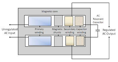
The ferroresonant transformer employs a rather unique magnetic structure that places a magnetic shunt leakage path between the primary and secondary windings. This structure is illustrated in Figure 2. This way only part of the transformer structure saturates at a higher fixed peak voltage level during each AC half cycle. When part of the core magnetically saturates, the primary and secondary windings are effectively decoupled. The AC capacitor on the secondary side resonates with existing inductance. This provides the carry-over energy to the load during this magnetically saturated phase, holding up the voltage level. The resulting waveform is a clipped sine wave with a fairly high level of harmonic distortion as a result. Some more modern designs include additional filtering that can bring the harmonic distortion down to just a few percent however.


Figure 2: Ferroresonant transformer structure

A ferroresonant transformer has some very appealing characteristics in addition to output voltage regulation:
  • Provides isolation from line spikes and noise that is normally coupled through on conventional transformers
  • Provides protection from AC line voltage surges
  • Provides carry over during momentary AC line drop outs that are of a fraction of a line cycle
  • Limits its output current if short-circuited
  • Extremely robust and reliable


Because of a number of other tradeoffs it is unlikely that you will find them in a DC power supply today. High frequency switching designs pretty much totally dominate in performance and cost. Ferroresonant transformer design tradeoffs include:
  • Large physical size
  • Relatively expensive and specialized
  • Limited to a specific line frequency as it resonates at that frequency


So, even though you are very unlikely to encounter a ferroresonant transformer in a DC power supply today, it’s interesting to see there still appears to be a healthy demand for ferroresonant transformers as AC line conditioners in a wide range of sizes, up to AC line power utility sizes.  Their inherent simplicity and robustness is hard to beat when long term, maintenance-free, reliable service is paramount, and AC line regulation in many regions around the world cannot be counted on to be well controlled.

Wednesday, September 5, 2012

Early Power Transistor Evolution, Part 2, Silicon


As discussed in part 1 of this two-part posting on early power transistor evolution, by the early 1960’s germanium power transistors were in widespread use in DC power supplies, audio amplifiers, and other relatively low frequency power applications. Although fairly expensive at that time the manufacturers had processes establish to reliably produce them in volume. To learn more about early germanium power transistors click here to review part 1.

As with most all things manufacturers continued to investigate ways of making things better, faster, and cheaper. Transistors were still relatively new and ready for further innovation. Next to germanium silicon was the other semiconductor in widespread use and with new and different processes developed for transistor manufacturing, silicon quickly displaced germanium as the semiconductor of choice for power transistors. One real workhorse of a power transistor that has truly stood the “Test of Time” is the 2N3055, pictured in Figure 1. Also pictured is his smaller brother, the 2N3054.


Figure 1: 2N3055 and 2N3054 power transistors

Following are some key maximum ratings on the 2N3055 power transistor:
  • VCEO = 60V
  • VCBO = 100V
  • VEBO= 7V
  • IC = 15A
  • PD = 115W
  • hfe= 45 typical
  • fT = 1.5 MHz
  • Thermal resistance = 1.5 oC/W
  • TJ= 200 oC
  • Package: TO-3 (now TO-204AA)
  • Polarity: NPN
  • Material/process: Silicon diffused junction hometaxial-base structure


Diffused junction silicon transistors made major inroads in the early 1960’s ultimately making the germanium power transistors obsolete.  One huge improvement using silicon, especially for power transistors, is the junction temperature, which is generally rated for 200 oC.  This allowed operating at much higher ambient temperatures and at higher power levels when compared to germanium. 

While the alloy junction process being used for the early germanium transistors favored making PNP transistors, the diffused junction process on silicon favored making NPN transistors somewhat more. Silicon diffused junction NPN transistors are much more prevalent than PNP devices, and the PNP complements to NPN devices, where available, are more costly.  

The diffusion process made a giant leap in transistor mass production possible. Many transistors could now be made at once on a larger silicon wafer, greatly reducing the cost. The more precise nature of the diffusion junction over the alloy junction also improved performance. As one example, tor the 2N3055 the transition frequency increased roughly another order of magnitude over the 2N1532 germanium alloy junction transistor in part 1, to 1.5 MHz.  

The hometaxial-base structure is a single simultaneous diffusion into both sides of a homogenously-doped base wafer, one side forming the collector and the other side the emitter. A pattern on the emitter side is etched away around the emitter, down to the P-type layer, to form the base. The emitter is left standing as a plateau or “mesa” above the base.

The 2N3054 was electrically identical to the 2N3055 except for its lower current and power capabilities. It’s smaller TO-66 package however was never very popular and was quietly phase out in the early 1980’s, sometimes along with some of the devices that were packaged in it!

Process improvements beyond the single diffused hometaxial-base structure continued through the 1960s with silicon transistors, including double diffused, double- and triple diffused planar and epitaxial structures. The epitaxial structure is a departure from the diffused structures in that features are grown onto the top of the base wafer. With greater control of doping levels and gradients, and more precise and complex geometries, the performance silicon power transistors continued to improve in most all aspects.

Plastic-packaged power transistors have for the most part come to displace hermetic metal packages like the TO-3 (TO-204AA), first due to the lower cost of the part and second, with simpler mounting, reducing the cost and labor of the products they are incorporated into. One drawback of most of the plastic-packaged power devices is their maximum temperature rating has been reduced to typically 150 oC, taking back quite a bit of temperature headroom provided by the same devices in hermetic metal packages. Sometimes there is a price to be paid for progress! Pictured in figure 2 are two (of many) popular power device packages, the smaller TO-220AB and the larger TO-247.

Figure 2: TO-220AB and TO-247 power device plastic packages

It’s pretty fascinating to see how transistors and the various processes used to manufacture them evolved over time. In these two posts I’ve hardly scratched the surface of the world of power transistors and power devices. For one there is a variety of other transistor types not touched upon, including a variety of power FETs. Power FETs have made major inroads in all kinds of applications in power supplies. Also work continues to provide higher power devices in surface mount packages. These are just a couple of numerous examples, possibly something to write about at a future date!


References: “RCA Transistor Thyristor & Diode Manual” Technical Series SC-14, RCA Electronic Components, Harrison, NJ 

Thursday, August 23, 2012

Early Power Transistor Evolution, Part 1, Germanium


We recently completed our “Test of Time” power supply contest. Contestants told us about how they were using their Harrison Labs/HP/Agilent DC power supplies and the older the power supply, the better. It was pretty fascinating to see the many innovative way these power supplies were being used. It was also fascinating to see so many “vintage” power supplies still functional and in regular use after many decades. Several of them even being vacuum tube based!

One key component found in most all power supplies from the mid 1950s on is, no surprise, power transistors. Shortly after manufacturers were able to make reliable and reasonably rugged transistors in the mid 1950s they also developed transistors that would handle higher currents and power. Along with higher power came the need to dissipate the power. This led to some interesting packaging; some familiar and others not as familiar. Hunting through my “archives” I managed to locate some early power transistors. In review of their characteristics it was quite enlightening to see how they evolved to become better, faster, and cheaper! I also found it is quite challenging to find good, detailed, and most especially, non-conflicting information on these early devices.

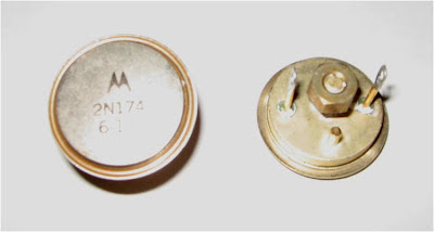
Germanium was the first semiconducting material widely adopted for transistors, power and otherwise. One early power transistor I came across was the 2N174, shown in Figure 1.


Figure 1: 2N174 Power Transistor

Following are some key maximum ratings on the 2N174 power transistor:

  •  VCEO = -55V
  • VCBO = -80V
  •  VEBO= -60V
  •  IC = 15A
  • PD = 150W
  • hfe= 25
  •  fT = 10 kHz
  •  Thermal resistance = 0.35 oC/W
  •  TJ= 100 oC
  • Package: TO-36
  • Polarity: PNP
  • Material/process: Germanium alloy junction

The alloy junction process provided a reliable means to mass produce transistors. Most of the earlier transistors are PNP with N type semiconductor “pellets” or “dots” of typically indium alloyed to a P type germanium wafer. This process favored PNP production as the indium had a lower melting point than the N-type germanium bases. Still, this was a relatively slow and expensive process as they were basically manufactured one at a time. These early alloy junction transistors were not passivated and therefore needed to be hermetically packaged to prevent contamination and degradation. Often referred to as a “door knob” package, the TO-36 stud mount package was quite a piece of work and was no doubt expensive to as a result. It had a pretty impressive junction-to-case thermal resistance but given the maximum temperature of just 100 oC, low thermal resistance was necessary in order to operate the transistor at a reasonable power level. The low maximum operating temperature of germanium was one of most limiting attributes, especially for power applications. The transition frequency, fT of just 10 kHz was also extremely low. This is the frequency where current gain, hfe, drops down to 1, ceasing to be an effective amplifier. The 2N174 appears to have originated in the later 1950’s.

Another early power transistor we used in our HP 855B bench power supplies is the 2N1532, as shown in Figure 2.


Figure 2: 2N1532 power transistors used in a Harrison Labs Model 855B power supply.

Following are some key maximum ratings on the 2N1532 power transistor:

  • VCEO = -50V 
  • VCBO = -100V
  • VEBO= -50V
  •  IC = 5A
  • PD = 94W
  • hfe= 20 to 40
  • fT = 200 kHz
  • Thermal resistance = 0.8 oC/W
  •  TJ= 100 oC
  • Package: TO-3
  • Polarity: PNP
  • Material/process: Germanium alloy junction
The 2N1532 is also a germanium PNP power transistor, similar to a number of other power transistors of the time. It is packaged in the widely recognizable TO-3 diamond-shaped hermetic package.  Being a much less complex case design it must have been considerably less costly than the TO-36 package in Figure 1, and has become one of the most ubiquitous hermetic power semiconductor packages of all times. To keep junction temperature rise down the Harrison Labs Model  855B power supply used three 2N1532 transistors in its series regulator to deliver just  18 volts and 1.5 amps output. It’s no wonder why these power supplies have stood the “Test of Time” as these transistors are running significantly de-rated, at just a fraction of their maximum power here.  It is also noteworthy to see the transition frequency of 200 kHz is 20 times that of the 2N174. This is one of the more questionable data I had found but if it is accurate then clearly design and process improvements contributed to this performance improvement.  While date codes on some of the capacitors in this model 855B power supply place its manufacture in 1962, early germanium PNP power transistors in TO-3 packages like these also typically originate back in the later 1950’s.

While germanium transistors have much greater conductivity, lower forward- and saturation voltage drops compared to silicon transistors, silicon ultimately won out in the end, especially for power transistor applications. Stay tuned for my second part in an upcoming posting. Discover how silicon evolved to rule the day for power transistors!

Tuesday, July 17, 2012

How Does a Power Supply regulate It’s Output Voltage and Current?


We have talked about Constant Voltage (CV) and Constant Current (CC) power supply operation in many various ways and applications here on the “Watt’s Up?” blog in the past. Indeed, CV and CC are fundamental operating modes of most all power supplies. But what exactly takes place inside the power supply that endows it with the ability to regulate either its output voltage or current, depending on the load? If you ever wondered about this, wonder no longer!

Most all power supplies regulate either their output voltage or output current at a constant level, depending on the load resistance relative to the power supply’s output voltage and current settings. This can be summarized as follows:

·         If R load > (V out / I out) then power supply is in CV mode
·         If R load < (V out / I out) then power supply is in CC mode

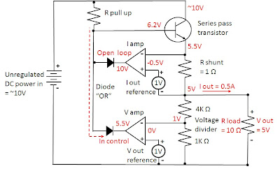
To accomplish this most all power supplies have separate voltage and current feedback control loops to limit either the output voltage or current, depending on the load. To illustrate this Figure 1 shows a circuit diagram of a basic 5 volt, 1 amp output series regulated power supply operating in CV mode.


Figure 1: Basic DC Power Supply Circuit, Constant Voltage (CV) Operation

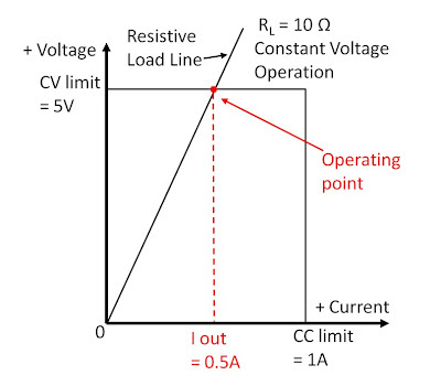
The CV and CC control loops/amplifiers each have a reference input value. In this case the reference values are both 1 volt. In order to regulate output voltage the CV error amplifier compares its 1 volt reference against a resistor divider that divides the output voltage down by a factor of 5, limiting the output voltage to 5 volts. Likewise the CC error amplifier compares its 1 volt reference against a 1 ohm current shunt resistor located in the output current path, limiting the output current to 1 amp. For Figure 1 the load resistance is 10 ohms. Because this load resistance is greater than (V out / I out) = 5 ohms, the power supply is operating in CV mode. The CV error amplifier takes control of the series pass transistor by drawing away excess base current from the series pass transistor, though the diode “OR” network. The CV amplifier is operating in closed loop, maintaining its error voltage at zero volts. In comparison, because the actual output current is only 0.5 amps the CC amplifier tries to turn the current on harder but cannot because the CV amplifier has control of the output. The CC amplifier is operating open loop. Its output goes up to its positive limit while it has -0.5 volts of error voltage. The output I-V diagram for this Constant Voltage operation is shown in Figure 2.


Figure 2: Power Supply I-V Diagram, CV Operation

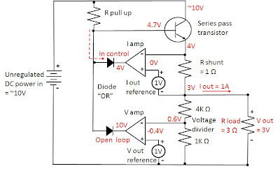
Now say we increase the load by lowering the output load resistance from 10 ohms down to 3 ohms. Figure 3 shows the circuit diagram of our basic 5 volt, 1 amp output series regulated power supply revised for operating in CC mode with a 3 ohm load resistor.


Figure 3: Basic DC Power Supply Circuit, Constant Current (CC) Operation

Because the load resistor is lower than (V out / I out) = 5 ohms, the power supply switches to CC mode. The CC error amplifier takes control when the voltage drop on the current shunt resistor increases to match the 1 volt reference value, corresponding to 1 amp output, drawing excess base current from the series pass transistor though the diode “OR” network. The CC amplifier is now operating closed loop, regulating the output current to maintain its input error voltage at zero. In comparison, because the actual output voltage is now only 3 volts the CV amplifier tries to increase the output voltage but cannot because the CC amplifier has control of the output. The CV amplifier is operating open loop. Its output now goes up to its positive limit while it has -0.4 volts of error voltage. The output I-V diagram for this Constant Current operation is shown in Figure 4.


Figure 4: Power Supply I-V Diagram, CC Operation

As we have seen most all power supplies have separate current and voltage control loops to regulate their outputs in either a Constant Voltage (CV) or in a Constant Current (CC) mode. One or the other takes control, depending on that the load resistance is in relation to what the power supply’s output voltage and current settings are. In this way both the load and power supply are protected by limiting the voltage and current that is delivered by the power supply to the load. By understanding this theory behind a power supply’s CV and CC operation it is also easier to understand the underlying reason for why various power supply characteristics are the way they are, as well as see how other power supply capabilities can be created by building on top of this foundation. Stay tuned!

Thursday, April 19, 2012

Experiences with Power Supply Common Mode Noise Current Measurements

I wrote an earlier posting “DC Power Supply Common Mode Noise Current Considerations” (click here to review) as common mode noise current can be an issue in electronic test applications we face. This is not so much of an issue with all-linear based power supply designs as it can be for ones incorporating switching based topologies. High performance DC power supplies designed for test applications should have relatively low common mode current by design. I thought this would be a good opportunity to get some more first-hand experience validating common mode noise current. The exercise proved to be a bit of an eye-opener. I tried different approaches and, no surprise; I got back seemingly conflicting results. Murphy was busy working overtime here!

I settled on a high performance, switching-based DC source on having a low common mode noise characteristic of 10 mA p-p and 1 mA RMS over a 20 Hz to 20 MHz measurement bandwidth. To properly make this measurement the general consensus here is a wide band current probe and oscilloscope is the preferred solution for peak to peak noise, and a wide band current probe and wide band RMS voltmeter is the preferred solution for RMS noise. As the wide band RMS voltmeters are pretty scarce here I relied on the oscilloscope for both values for the time being. The advantages of current probes for this testing are they provide isolation and have very low insertion impedance.

I located group’s trusty active current probe and oscilloscope. The low signal level I intended to measure dictated using the most sensitive range providing 10 mA/div (with oscilloscope set to 10 mV/div).
One area of difficulty to anticipate with modern digital oscilloscopes is there are a lot of acquisition settings to contend with, all having a major impact on the actual reading. After sorting all of these out I finally got a base line reading with my DC source turned off, shown in Figure 1.

Figure 1: Common mode noise current base-line reading

My base-line reading presented a bit of a problem. With 1 mV corresponding to 1 mA my 2.5 mA p-p / 0.782 mA RMS base-line values were a bit high in comparison to my expected target values. It would be nicer for this noise floor to be at about 10X smaller so that I don’t have to really factor it out. Resorting to the old trick of looping the wire through the current probe 5 times gave me a 5X larger signal without changing the base-line noise floor. The oscilloscope was now displaying 2 mA /div, with 1 mV corresponding to 0.2 mA. In other words my base-line is now 0.5 mA p-p / 0.156 mA RMS. The penalty for doing this is of course more insertion impedance. Now I was all set to measure the actual common mode noise current. Figure 2 shows the common mode noise current measurement with the DC source on.

Figure 2: Common mode noise current measurement

Things to pay attention to include checking the current on both + and – leads individually to earth ground and load the output with an isolated load (i.e. a power resistor). Full load most often brings on worst case values. Based on the 0.2 conversion ratio I’m now seeing 8 mA p-p and 1.12 mA RMS, including the baseline noise. I am reasonably in the range of the expected values and having a credible measurement!

I decided to compare this approach to making a 50 ohm terminated direct connection. This set up is depicted in Figure 3 below.
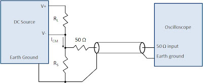
Figure 3: 50 ohm terminated directly connected common mode noise current measurement

I knew insertion impedance was considerably more with this approach so I tried both 10 ohm and 100 ohm shunt values to see what kind of readings I would end up with. Table 1 summarizes the results for the directly connected measurement approach.

Table 1: 50 ohm terminated directly connected common mode noise current results

Clearly the common mode noise current results were nowhere near what I obtained with using a current probe, being much lower, and also highly dependent on the shunt resistor value. Why is that? Looking more closely at the results, the voltage values are relatively constant for both shunt resistor cases. Beyond a certain level of increasing shunt resistance the common mode noise behaves more as a voltage than a current. For this particular DC source the common mode voltage level is extremely low, just a few millivolts.

Not entirely content with the results I was getting I located a different high performance DC source that also incorporated switching topology. No actual specifications or supplemental characteristics had been given for it. When tested it exhibited considerably higher common mode noise than the first DC source. The results are shown in table 2 below.

Table 2: 50 ohm terminated directly connected common mode noise current results, 2nd DC source

With both voltage and current results changing for these two test conditions the common mode noise is exhibiting somewhere between being a noise current versus being a noise voltage. I had hoped to see what the results would be using the current probe but it seemed to have walked away when I needed it!

In Summary:
Making good common mode current noise measurements requires paying a lot of attention to the choice of equipment, equipment settings, test set up, and DUT operating conditions. I still have bit more to investigate but at least I have a much better understanding as to what matters. Maybe in a future posting I can provide what could be deemed as the “golden set up”! To get results that correlate reasonably with any stated values will likely require a set up that exhibits minimal insertion impedance across the entire frequency spectrum. Making directly coupled measurements without the use of a current probe will prove challenging except maybe for DC sources having rather high levels of common mode noise currents

The underlying concern here of course is what is what will be the impact to the DUT due to any common mode noise current from the test system’s DC source. Generally that is any common mode noise current ends up becoming differential mode noise voltage on the DUT’s power input due to impedance imbalances. But one thing I found from my testing is that the common mode noise is not purely a current with relatively unlimited compliance voltage but somewhere between being a noise voltage and noise current, depending on loading conditions. For the first DC source, with what appears to be only a few millivolts behind the current it is unlikely that it would create any issues for even the most sensitive DUTs. For the second DC source however, having 100’s of millivolts behind its current, could potentially lead to unwanted differential voltage noise on the DUT. Further investigation is in order!

Friday, February 17, 2012

The economics of recharging your toy helicopter

While on a business trip visiting customers in Taiwan back in December, I got a toy helicopter as a thank-you gift from one of my coworkers (thanks, Sharon!). This toy helicopter is fun to fly and is surprisingly stable in the air.


Flight time is about 7 minutes, and the battery recharge time is about 40 minutes. It can be recharged from a powered USB port by using a wire that came with the toy that has a USB connector on one end and the helicopter charging connector on the other end. Or, it can be recharged from the six AA alkaline batteries inside the handheld controller via a wire that exits from the controller. Thinking I did not want to prematurely drain the controller batteries, I typically used the USB charging method by using my iPad’s 10 W USB power adapter plugged into a wall outlet. So I got to thinking about which charging method was more economical: charging from a wall outlet or from the batteries. Luckily, I have test equipment at my disposal that can help me answer that question!


Recharging using AC power via USB power adapter
Using one of our Agilent 6812B AC sources, I captured the AC power used during a recharge cycle. I used the AC source GUI to take readings of power every second for the charge period and plotted it in a spreadsheet (graph shown below). I found that the power consumed started at about 2.2 W and ended at about 1.2 W roughly 41 minutes later. The energy used during this time was 1.1 W-hours. Where I live in New Jersey, the utility company charges about 15 cents per kilowatt-hour, so 1.1 W-hours of energy used to charge the helicopter costs fractions of a penny (0.0165 cents = US$ 0.000165). This is basically nothing!


Recharging using controller battery power
To analyze the current drawn from the controller batteries, I used one of our Agilent N6705B DC power analyzers with an N6781A SMU module installed. I ran the battery current path through the SMU set for Current Measure mode and used our 14585A Control and Analysis software. I captured the current drawn from the six AA batteries in the controller during the helicopter recharge cycle. These batteries are in series, so the same current flows through each of the six batteries and also through the SMU for my test.


For the recharge period (about 43 minutes using this method), the software shows the batteries provided 173 mA-hours of charge to the helicopter. A typical AA alkaline battery is rated for 2500 mA-hours, so that means I would get about 14 (= 2500/173) charge cycles from these six batteries. If you shop around for high-quality AA batteries, you might find them for as low as 25 cents per battery. Since the controller takes six of these, the battery cost for the controller is $1.50. If I can recharge the helicopter 14 times with $1.50 worth of batteries, each recharge cycle costs about 10.7 cents (= US$ 0.107). This is 650 times more expensive than using the AC power method, so I will continue using the wall outlet to recharge my toy helicopter! How about you?
Note that with the AC power recharge method, you pay for the kilowatt-hours you consume from your utility company. With the controller battery power method, you pay for the mA-hours you consume from your batteries. Consider this: if you choose the AC power method, you will save US$ 0.106835 per recharge cycle. That means after just 2.81 million recharge cycles, you will have saved enough money to buy yourself a real helicopter worth US$ 300,000, so you better get started now!

Tuesday, December 6, 2011

Should I Use a Switching or Linear DC Power Supply For My Next Test System? (part 4 of 4)

Part 4 of 4: Making the Comparison and Choice
In the first three parts of this post we looked at the topologies and merits of linear DC power supplies, traditional and high-performance switching DC power supplies, and common mode noise current considerations of each. So now in this final part we have reached a point where we can hopefully make an informed comparison and choice. Tables 1 and 2 summarize several key qualitative and quantitative aspects of all three DC power supply types, based on what we have learned.
Table 1: Qualitative comparison of DC power supply topologies

Table 2: Quantitative comparison of DC power supply topologies

So what DC power supply topology is the best choice for your next test system? In the past it usually ended up having to be a linear topology to meet performance requirements in most all but very high power, lower performance test situations. However, high-performance switching DC power supplies have nowadays for the most part closed the performance gap with linear DC power supplies. And, at higher power, the favorable choice may come down to selecting between several different switching DC power supplies only, due to their cost, size, and availability. So the answer is you need to make a choice based on how well the power supply meets your performance, space, and cost requirements, rather than basing the choice on its topology. Except for the most demanding low power test applications, like those needing the performance of a source measure unit (SMU), chances are much higher these days that the next DC power supply you select for your next test system you will be a switcher (and you possibly may not even realize it). What has been your experience?

Tuesday, November 29, 2011

Should I Use a Switching or Linear DC Power Supply For My Next Test System? (part 3 of 4)

Part 3 of 4: DC Power Supply Common Mode Noise Current Considerations
Common mode noise current is a fact of life that manifests itself in many ways in test systems. There are several mechanisms that couple unwanted common mode noise currents into ground loops. An excellent overview on this is given in a two part post on the General Purpose Test Equipment (GPETE) blog “Ground Loops and Other Spurious Coupling Mechanisms and How to Prevent Them” (click here). However this is also an important consideration with our choice of a DC system power supply for testing as they are a source of common mode noise current. This is one area where linear DC power supplies still outperform switching DC power supplies. This can become a concern in some highly noise-sensitive test applications. As shown in Figure 1 the common mode noise current ICM is a noise signal that flows out of both output leads and returns through earth. By nature it is considered to be a current signal due to its relatively high associated impedance, ZCM.

Figure 1: Common Mode Noise Current and Path

Common mode noise current is often much greater in traditional switching DC power supplies. High voltage slewing (dv/dt) of the switching transistors capacitively couples through to the output, in extreme cases generating up to hundreds of milliamps pk-pk of high frequency current. In comparison, properly designed linear DC power supplies usually generate only microamps pk-pk of common mode noise current. It is worth noting even a linear DC power supply is still capable of generating several milliamps pk-pk of common mode noise current, if not properly designed. High-performance switching DC power supplies are much closer to the performance of a linear. They are designed to have low common mode noise current, typically just a few milliamps.

Common mode noise current can become a problem when it shows up as high frequency voltage spikes superimposed on the DC output voltage. This depends on the magnitude of current and imbalance in impedances in the path to the DUT. If large enough, this can become more troublesome than the differential mode noise voltage present. Generally, the microamp level of a linear DC power supply is negligible, while hundreds of milliamps from a traditional switching DC power supply may be cause for concern. Because common mode noise current is often misunderstood or overlooked, one may be left with a false impression that all switching DC power supplies are simply unsuitable for test, based on a bad experience with using one, not being aware that its high common mode noise current was actually the underlying cause.

In practice, at typical levels, common mode noise current often turns out not to be an issue. First, many applications are relatively insensitive to this noise. For example, equipment in telecommunications and digital information systems are powered by traditional switching DC power supplies in actual use and are reasonable immune to it. Second, where common mode noise current is more critical, the much lower levels from today’s high-performance switching DC power supplies makes it a non-issue in all but the most noise sensitive applications.

In those cases where common mode noise current proves to be a problem, as with some extremely sensitive analog circuitry, adding filtering can be a good solution. You can then take advantage of the benefits a switching DC power supply has to offer. A high-performance switching DC power supply having reasonably low common mode current can usually be made to work without much effort in extremely noise-sensitive applications, using appropriate filtering, capable of attenuating the high frequency content present in the common mode noise current. Such filtering can also prove effective on other high frequency noises, including AC line EMI and ground loop pickup. These other noises may be present regardless of the power supply topology.

Coming up next is the fourth and final part where we make our overall comparison and come to a conclusion on which power supply topology is best suited for test.

References:
1. Taking The Mystery Out Of Switching-Power-Supply Noise Understanding the source of unspecified noise currents and how to measure them can save your sanity
By Craig Maier, Hewlett Packard Co. © 1991 Penton Publishing, Inc.

Wednesday, November 23, 2011

Should I Use a Switching or Linear DC Power Supply For My Next Test System? (part 2 of 4)

Part 2 of 4: Switching DC system power supply attributes
In part 1 we looked at the topology and merits of a linear DC power supply. To be fair we now have to give equal time to discuss the topology and merits of a switching DC system power supply, to make a more informed choice of what will better suit our needs for powering up and testing our devices.

Traditional switching DC power supply topology
The basic traditional switching power supply depicted in Figure 2 is a bit more complex compared to a linear power supply:
1. The AC line voltage is rectified and then filtered to provide an unregulated high voltage DC rail to power the following DC-to-DC inverter circuit.
2. Power transistors switching at 10’s to 100’s of kHz impose a high voltage, high frequency AC pulse waveform on the transformer primary (input).
3. The AC pulse voltage is scaled by the transformer turns ratio to a value consistent with the required DC output voltage.
4. This transformer secondary (output) AC voltage is rectified into a pulsed DC voltage.
5. An LC (inductor-capacitor) output filter averages the pulsed voltage into a continuous DC voltage at the power supply’s output.
6. As with a linear power supply, an error amplifier compares the DC output voltage against a reference to regulate the output at the desired setting.
7. A modulator circuit converts the error amplifier signal into a high frequency, pulse width modulated waveform to drive the switching power transistors.


Figure 2: Basic switching DC power supply circuit

In spite of being more complex the key thing is its much higher operating frequency, several orders of magnitude over that of a linear power supply, greatly reduces the size of the magnetic and filtering components. As a result traditional switching DC power supplies have some inherent advantages:
• High power conversion efficiency of typically 85%, relatively independent of output voltage setting.
• Small size and lightweight, especially at higher power.
• Cost effective, especially at higher power.

Traditional switching DC power supplies also have some typical disadvantages:
• High output noise and ripple voltage
• High common mode noise current
• Slow transient response to AC line and DC output load changes.


High-performance switching DC power supplies lessen the gap
Traditional switching DC power supply performance is largely a result of optimizing well established switching topologies for cost, efficiency and size, exactly the areas where linear DC power supplies suffer. Performance generally had been a secondary consideration for switching DC power supplies. However, things have now improved to better address the high-performance needs for electronics testing. Incorporating more advanced switching topologies, careful design, and better filtering, high-performance switching DC power supplies compare favorably with linear DC power supplies on most aspects, while still retaining most of the advantages of switchers.

So our choice on whether to use a linear or switching power supply has now gotten a bit more difficult! One area that still differentiates these DC power supply topologies is common mode current noise, worthy of its own discussion, which is exactly what I will do in part 3, coming up next!

Tuesday, November 15, 2011

Should I Use a Switching or Linear DC Power Supply For My Next Test System? (part 1 of 4)

Part 1 of 4: Linear System DC Power Supply Attributes
To kick things off I thought it would be helpful to start with a short series of posts discussing something fundamental we’re often faced with; that is making the choice of whether to use a switching or linear DC power supply to power up our devices under test. In part 1 here I’ll begin my discussion with the topology and merits of linear DC power supplies, as I have heard countless times from others that only a linear power supply will do for their testing, principally due to its low output noise. Of course we do not want to take the chance of having power supply noise affect our devices’ test results. While I agree a linear DC power supply is bound to have very low noise, a well-designed switching DC power supply can have surprisingly good performance. So the choice may not be as simple anymore. The good thing here however is this may give us a lot more to choose from, something that may better meet our overall needs, including size and cost, among other things.

Linear DC Power Supply Topology
A linear DC power supply as depicted in Figure 1 is relatively simple in concept and in basic implementation:
  1. A transformer scales the AC line voltage to a value consistent with the required maximum DC output voltage level.
  2. The AC voltage is then rectified into DC voltage.
  3. Large electrolytic capacitors filter much of the AC ripple voltage superimposed on the unregulated DC voltage.
  4. Series-pass power transistors control the difference between the unregulated DC rail voltage and the regulated DC output voltage. There always needs to be some voltage across the series pass transistors for proper regulation.
  5. An error amplifier compares the output voltage to a reference voltage to regulate the output at the desired setting.
  6. Finally, an output filter capacitor further reduces AC output noise and ripple, and lowers output impedance, for a more ideal voltage source characteristic.

Figure 1: Basic Linear DC Power Supply Topology

Linear DC power supply design is well established with only incremental gains now being made in efficiency and thermal management, for the most part. Its straightforward configuration, properly implemented, has some inherent advantages:

  • Fast output transient response to AC line and output load changes
  • Low output noise and ripple voltage, and primarily having low frequency spectral content
  • Very low common mode noise current
  • Cost competitive at lower output power levels (under about 500 watts)

It also has a few inherent disadvantages:

  • Low power efficiency, typically no better than 60% at full output voltage and decreases with lower output voltage settings
  • Relatively large physical size and weight
  • High cost at higher power (above about 500 watts)

So it sounds like a linear power supply has to be the hands-down winner especially for low power applications. Or not? To make a more-informed choice we need to look at the topology and merits of a switching power supply, which I will be doing in part 2!