Showing posts with label constant voltage. Show all posts

Monday, March 23, 2015

Use slew rate control to cleanly power up and reduce peak inrush current of your DUTs

Previously on Watt’s Up? a colleague wrote about how the current limit setting affects a power supply’s voltage response time (click here to review). In this posting he clearly shows how a low current limit setting can greatly slow down the output voltage turn on response time when powering up your DUT.

While this is generally true and good advice, especially for basic performance power supplies, there are additional things to consider when working with high performance power supplies models, as you will see.

Many basic performance power supplies tend to have larger output filter capacitors in order to achieve lower output noise performance. A disadvantage of having a large output capacitor is that it slows down the output voltage response speed of the power supply. Basic performance power supplies can have turn on response times on the order of a 100 milliseconds.

High performance power supplies operate by a somewhat different set of rules. In comparison to basic performance power supplies they typically have much smaller output capacitors and they are designed to have output turn on and turn off response times on the order of a millisecond or less.

However, absolute fastest is not always the best and that is why fast, high performance power supplies also usually incorporate an output voltage slew rate control as well. This allows you to optimize the output turn on and turn off speed for your particular application. This lets you take advantage of the faster output speed you have available, without it being overkill and cause other problems.

The two most common problems that arise when powering up and powering down many DUTs are related to charging and discharging the input filter capacitor incorporated into them. They are:
  • High peak inrush (and discharge) currents due to the high dV/dt slew rate being applied
  • Power supply CC-CV mode cross over issues resulting from the high peak inrush current


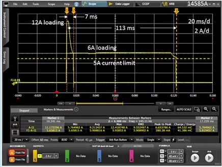
To illustrate, the turn on characteristic of our N6762A power supply was captured when powering up a load consisting of a 1,200 microfarad capacitor in parallel with a 10 ohm resistor. The N6762A was set to 10 volts and its voltage slew rate set to maximum.  This was captured using the N6762A’s digitizing voltage and current readback together with the 14585A software, shown in Figure 1.


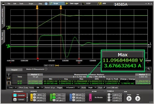
Figure 1: N6762A power supply turn on response set to maximum slew rate into parallel RC load

The vertical markers have been placed at zero and maximum voltage points of the turn on ramp. The peak inrush current reaches 3.7 amps and the peak voltage overshoots to 11.06 volts, 10% over the 10 volt setting. The overshoot is a result of the power supply crossing over into current limit during the ramp up and allowing the voltage to rise to 11.06 volts before the voltage control loop regains control to bring the output back down to 10 volts. It also takes a little while for the voltage to settle after the peak overshoot. Both the overshoot voltage and peak inrush current can be problems when powering up a DUT. These occur as a result of having too fast of a voltage slew rate when powering the DUT.

To address the problem we then set the N6762A’s slew rate to a more acceptable value of 2,000 volts/second. The turn on voltage and current were again captured and are shown in Figure 2. As can be seen the voltage overshoot is eliminated and the inrush current has been reduced to a more moderate 3.3 amps.


Figure 2: N6762A power supply turn on response set to 2,000 V/s slew rate into parallel RC load

So in closing high performance power supplies have a significant advantage in their output response speed, in comparison to basic power supplies. And while faster is usually better, absolute fastest may not be best, and this applies to the output response time of power supplies as well! But by having the ability to set the output slew rate on high performance power supplies gives you the ability to optimize its speed for your given application, providing for the best possible outcome possible!

.

Tuesday, November 18, 2014

Why does the response time of OCP vary on the power supply I am using and what can I do about it? Part 1

In a previous posting of mine “Providing effective protection of your DUT against over voltage damage during test”(click here to review), an important consideration for effective protection was to factor in the response time of the over voltage protect (OVP) system. Due to the nature of over voltage damage, the OVP must be reasonably fast. The response time can typically be just a few tens of microseconds for a reasonably fast OVP system on a higher performance system power supply to hundreds of microseconds on a more basic performance system power supply. This response time usually does not vary greatly with the amount of over voltage being experienced.

Just as with voltage, system power supplies usually incorporate over current protect (OCP) systems as well. But unlike over voltage damage, which is almost instantaneous once that threshold is reached, over current takes more time to cause damage. It also varies in some proportion to the current level; lower currents taking a lot longer to cause damage. The I2t rating of an electrical fuse is one example that illustrates this effect.

Correspondingly, like OVP, power supply OCP systems also have a response time. And also like OVP, the test engineer needs to take this response time into consideration for effective protection of the DUT.  However, unlike OVP, the response time of an OCP system is quite a bit different. The response time of an OCP system is illustrated in Figure 1.


Figure 1: Example OCP system response time vs. overdrive level

Here in Figure 1 the response time of the OCP system of a Keysight N7951A 20V, 50A power supply was characterized using the companion 14585A software. It compares response times of 6A and 12A loading when the current limit is set to 5A. Including the programmed OCP delay time of 5 milliseconds it was found that the actual total response time was 7 milliseconds for 12A loading and 113 milliseconds for 6A loading.

This is quite different than the response time of an OVP system. Even if the OCP delay time was set to zero, the response is still on the order of milliseconds instead of microseconds for the OVP system. And when the amount of overdrive is small, as is the case for the 6A loading, providing just 1A of overdrive, the total response time is much greater. Why is that?

Unlike the OVP system, which operates totally independent of the voltage limit control system, the OCP system is triggered off the current limit control system. Thus the total response time includes the response time of the current limit as well. The behavior of a current limit is quite different than a simple “go/no go” threshold detector as well. A limit system, or circuit, needs to regulate the power supply’s output at a certain level, making it a feedback control system. Because of this stability of this system is important, both with crossing over from constant voltage operation as well as maintaining a stable output current after crossing over. This leads to the slower and overdrive dependent response characteristics that are typical of current limit systems.

So what can be done about the slower response of an OCP system? Well, early on in this posting I talked about the nature of over current damage. Generally over current damage is much slower by nature and the over drive dependent response time is in keeping with time dependent nature of over current damage. The important thing is understand what the OCP response characteristic is like and what amount of over current your DUT is able to sustain, and you should be able to make effective use of the over current protection capabilities of your system power supply.

If however you are still looking how you might further improve on OCP response speed, look for my follow up to this in my next posting!

Wednesday, August 20, 2014

Some differences between constant current (CC) and constant resistance (CR) loading on your DUT’s performance

Most electronic loads provide constant current (CC), constant resistance (CR) and constant voltage (CV) loading. Some also offer constant power (CP) loading as well. The primary reason for this is this gives the test engineer a choice of loading that best addresses the loading requirement for the DUT, which invariably is some kind of power source.

Most usually the device should be tested with a load that reflects what the loading is like for its end use. In the most common case of a device being predominantly a voltage source the most common loading choices are either CC or CR loading, which we will look at in more detail here. Some feel they can be used interchangeably when testing a voltage source. To some extent this is true but in some cases only one or the other should be used as they can impact the DUT’s performance quite differently.

Let’s first consider static performance. In Figure 1 we have the output characteristics of an ideal voltage source with zero output resistance (a regulated power supply, for example) and a non-ideal voltage source having series output resistance (a battery, for example).  Both have the same open circuit (no load) voltage. Superimposed on these two source output characteristics are two load lines; one for CC and one for CR. As can be seen they are set to draw the same amount of current for the ideal voltage source. However, for the non-ideal voltage source, while the CC load still continues to draw the same amount of current in spite of the voltage drop, not surprisingly the CR load draws less current due to its voltage-dependent nature.


Figure 1: CC and CR loading of ideal and non-ideal voltage sources

CC loading is frequently used for static power supply tests for a key reason. Power supplies are usually specified to have certain output voltage accuracy for a fixed level of current. Using CC loading assures the loading condition is met, regardless of power supply’s output voltage being low or high, or in or out of spec. Non-ideal voltage sources, like batteries, present a little more of a problem and are often specified for both CC and CR loading as a result, to reflect the nature of the loading they may be subjected to in their end use. Due to a battery's load-dependent output voltage, trying to use one type of loading in place the other becomes an iterative process of checking and adjusting loading until the acceptable operating point is established.

Let’s now consider dynamic performance.  CC loading generally has a greater impact on a power supply’s ability to turn on as well as its transient performance and stability, in comparison to CR loading. When the power supply first starts up its output voltage is at zero. A CR load would demand zero current at start up. In comparison a CC load still demands full current. Some power supplies will not start up properly under CC loading. With regard to transient response and stability, CR loading provides a damping action, increasing current demand when the transient voltage increases and decreases demand when the transient voltage decreases, because the current demand is voltage dependent. CC loading does not do this, which can negatively influence transient response and stability somewhat. Whether CC or CR loading is used depends on what the power supply’s specifications call out for the test conditions. Batteries have some dynamic considerations as well. Their output response can be modeled as a series of time constants spanning a wide range of time. This presents somewhat of a moving target for an algorithm that uses an iterative approach to settling on an acceptable operating point.


This is just a couple of examples of how a load’s characteristic affects the performance of the device it is loading, and why electronic loads have multiple operating modes to select from, and worth giving thought next time towards how your device is affected by its loading!

Wednesday, January 29, 2014

Using a DC Power Supply to Regulate Energy

In a previous 2-part posting I talked about what power and energy is (part 1 – energy) (part 2 – power).  It is pretty straight-forward thing to do to use a DC power supply for regulating voltage or current. Constant voltage (CV) and constant current (CC) regulation are standard features of most all DC power supplies used in testing. However, what if you have an unusual application calling for applying a fixed amount of energy to your device under test (DUT)? For example, adding a fixed amount of energy to a calorimeter or chemical process, or testing the must (or must not) tripping energy of a fuse, or circuit breaker, or squib or detonator perhaps?

When the resistance of a device remains constant, it is relatively straight-forward to apply a fixed amount of energy to a DUT. By applying a fixed voltage or current, the power in the DUT remains constant. Then the energy is simply:

E = (V2/R)*t = (I2*R)*t

Where E is the energy in watt-seconds or joules, V is voltage in volts, R is resistance in ohms, I is the current in amps, and t is time in seconds. All you now need to do is apply the constant voltage or current for a pre-determined amount of time and you will then be delivering a fixed amount of energy to your DUT.

Many times however, a lot of DUTs do not maintain constant loading. The may have a dynamically varying loading by nature or its resistance dramatically increases as it heats up. How do you regulate a fixed amount of energy to your DUT under these circumstances? One possibility is to use one of a few specialized power supplies on the market can regulate their outputs with constant power. As the DUT’s loading decreases or increases the power supply will adjust its output accordingly in order to maintain a constant output power delivered to the DUT.  Again then, by applying this constant power for a pre-determined amount of time you will then be delivering a fixed amount of energy to your DUT.

Still, for DUTs that do not maintain constant loading, it is very often not desirable, or outright unacceptable, to apply constant power sourcing.. It may be you can only apply a fixed voltage or current to your DUT. What can you do for these circumstances? Time can no longer remain a fixed value when trying to regulate a fixed amount of energy. The solution becomes quite a bit more complex, as depicted in Figure 1.


Figure 1: Regulating a fixed amount of energy to a DUT

Putting the solution depicted in Figure 1 into practice can prove challenging. The watt-hour meter needs to provide a trigger out signal when the desired watt-hour (or watt-second) threshold level is reached. This becomes even more challenging if this response time required needs to be just fractions of a second for this set up. More than likely this may become a piece of customized hardware.

Interestingly this very set up can be programmatically configured within our N6900A and N7900A series Advanced Power System (APS) power supplies. These products have Amp-hour and Watt-hour measurement integrated into their measurement systems. Not only can you measure these parameters, there is a programmable way to act on them in a variety of ways as well, which is the expression signal routing. Logical expressions can be programmed and downloaded into APS, which then acts on them at hardware-level speeds.  Creating and loading the signal routing expression into the APS unit is simplified by using the N7906A Power Assistance software, which let me do it graphically, as shown in Figure 2.


Figure 2: Graphically developing and loading an energy limit setting into an Agilent APS unit

In Figure 2 a threshold comparator was set to generate a trigger output at a level of 0.0047 watt-hours. This trigger was then routed to the output transient system, to cause the output to transition to a new output level when triggered. I had entered in zero volts as the triggered output level. Thus when the watt-hour reading reached its trigger point, the output went to zero, cutting off any more power and energy from being delivered to the DUT.

The SCPI command set for this signal routing expression is also generated from this software utility by clicking on “SCPI to clipboard”. This saves on the effort generating the code manually if you are incorporating the expression into a larger test program. For this expression the code generated is:

:SENSe:THReshold1:FUNCtion WHOur
:SENSe:THReshold1:WHOur 0.0047
:SENSe:THReshold1:OPERation GT
:SYSTem:SIGNal:DEFine EXPRession1,"Thr1"
:TRIGger:TRANsient:SOURce EXPRession1


To test things out a 1.18 ohm resistive load was used to draw 84.75 watts for a 10 volt output setting. The output cut back to zero volts at nearly 200 milliseconds, as expected. This is shown in the oscilloscope capture in Figure 3.


Figure 3: APS output for an 84.75 watt load and energy limit set to 0.0047 watt-hours

The load power was then doubled by increasing the output voltage to 14.142 volts. The APS output cut back to zero volts in half the time, delivering the same amount of energy, as expected. This is depicted in the oscilloscope capture in Figure 4.


Figure 4: APS output for a 169.5 watt load and energy limit set to 0.0047 watt-hours

While using a resistor makes it easy to see that a set amount of energy is being delivered to the load. However, being able to act on a real time watt-hour energy measurement makes it very practical to do deliver a fixed amount of energy, regardless of the dynamic nature of the load over time.

Wednesday, November 6, 2013

Paralleling power supplies for more power without compromising performance!

A year ago my colleague here, Gary, provided a posting “How can I get more power from my power supplies?” (Click here to review). He describes connecting power supplies in series for higher voltage or in parallel for higher current. Along with suggested set ups a list of requirements and precautions are also provided.

Connecting multiple power supplies in parallel operating as voltage sources is always problematic as there will be some imbalance of voltage between them. That’s why, in this previous posting, one unit operates as a voltage source and the remaining paralleled units operate in constant current. The compliance voltage limit of all the units operating in constant current need to be set higher than the master in operating in constant voltage in order to maintain this operation. This is illustrated in Figure 1.


Figure 1: Operating power supplies in parallel for higher power


As long as a high level of loading is maintained the paralleled units remain in their respective operating modes (in this case at least 2/3 loading). However, what happens if you cannot maintain that high level of loading? It is possible in practice to operate at lighter loads with this approach. In this case it is important to set the voltage levels of all the units the same. Now what happens is when the units are fully loaded they operate as already described, with the lowest voltage unit remaining in constant voltage. But when they are unloaded the lower voltage units transition to unregulated operation and the highest voltage unit then maintains the overall output in constant voltage. This is shown in Figure 2, for 0 to 1/3 loading.


Figure 2: Conditions of power supplies connected in parallel at light loading

There is a bit of performance compromises as a result. The transition between the lowest and highest voltage limits adds to the voltage regulation. Also, due to different units experiencing mode crossover transitions between constant voltage, constant current and unregulated operating modes transient voltage performance suffers considerably.

An improvement on this direct paralleling approach is having a master-slave arrangement with control signals to maintain current sharing across units. Our N5700A and N8700A series power supplies use such a control arrangement as depicted in Figure 3, taken from the N5700A user’s guide.


Figure 3: N5700A Connection for parallel operation (local sensing used)

With this arrangement the master unit, operating in constant voltage, provides an analog current programming output signal to the slave unit, operating in constant current. In this way the two units equally share the load current across a wide range of load current.

Still, having multiple units with only one in constant voltage does not provide as good of dynamic performance as a single voltage source of higher power.  A unique and innovative approach was taken with our N6900A / N7900A series Advance Power System (APS) to support seamless parallel operation without compromising performance. The paralleling arrangement for our N6900A / N7900A series APS is depicted in Figure 4.


Figure 4: N6900A / N7900A series APS Connection for parallel operation

The N6900A / N7900A series APS paralleling arrangement also uses an analog control signal for driving current sharing. However with this arrangement there is no master or slaves. All units remain in constant voltage while equally sharing current. This provides the user with an easy way to scale a power system as required without having to worry about compromising performance.

Friday, July 12, 2013

Why have multiple output range DC power supplies?

Most often DC power supplies have a rectangular output characteristic, as depicted in figure 1. With an increasing load they output a fixed output voltage up to the current limit, at which point the voltage drops in order to maintain the current fixed at its limit.


Figure 1: DC power supply rectangular output characteristic.

There is however DC power supplies that offer multiple output ranges. One example of a multiple (dual in this case) output range DC power supply is our N678xA series DC source measure modules. Their output characteristics are depicted in Figure 2.


Figure 2: Agilent N678xA series source measure modules output characteristics

Unlike the output characteristic of a single output range DC power supply, you cannot get both the maximum current and maximum voltage of a multiple output range DC power supply at the same time.

What is the purpose of having multiple output ranges on a DC power supply?
There are times, especially when having to test a variety of devices, the need for greater current or voltage, but not necessarily needing both maximum voltage and current at the same time.  In these situations many times these test power needs are better served by a DC power supply having multiple output ranges. The advantages of a multiple output range DC power supply are smaller size, less power dissipation, and less input power required, in comparison to a single output range DC power supply of comparable voltage and current capability. If the N678xA series DC source measure modules had a single output range they would need to have a 60 watt output to cover the span of voltage they now provide with 20 watts of output power.  An even more extreme example is our B2900 series source measure units. They output up to 31.8 watts continuously, but can provide up to 210 volts and up to 3.03 amps over three output ranges.

The downside of having multiple output ranges is somewhat greater complexity. Figure 3 depicts a conceptual design for a dual output range DC power supply. 


Figure 3: Conceptual dual output range DC power supply

Because the transformer efficiently converts AC power by square of its turn ratio there is very little impact on its size to accommodate secondary windings with multiple taps or multiple secondary windings that can be alternately connected in series or parallel, in order to accommodate multiple output power ranges. Similarly, the linear series pass element dissipates about the same maximum power whether it is operating at a higher voltage with lower current, or at a lower voltage with a higher current.  

The end result is a multiple range DC power supply can provide a greater range of voltages and currents for a given output power at the expense of a little greater complexity. Often this is far preferable to the alternative of a much higher power, and larger single output range DC power supply!

Thursday, June 20, 2013

How can I measure output impedance of a DC power supply?

In my last posting “DC power supply output impedance characteristics”, I explained what the output impedance characteristics of a DC power supply were like for both its constant voltage (CV) and constant current (CC) modes of operation. I also shared an example of what power supply output impedance is useful for. But how does one go about measuring the output impedance of a DC power supply over frequency, if and when needed?

There are a number of different approaches that can be taken, but these days perhaps the most practical is to use a good network analyzer that will operate at low frequencies, ranging from 10 Hz up to 1 MHz, or greater, depending on your needs. Even when using a network analyzer as your starting point there are still quite a few different variations that can be taken.

Measuring the output impedance requires injecting a disturbance at the particular frequency the network analyzer is measuring at. This signal is furnished by the network analyzer but virtually always needs some amount of transformation to be useful. Measuring the output impedance of a voltage source favors driving a current signal disturbance into the output. Conversely, measuring the output impedance of a current source favors driving a voltage signal disturbance into the output. The two set up examples later on here use two different methods for injecting the disturbance.

The reference input “R” of the network analyzer is then used to measure the current while the second input “A” or “T” is used to measure the voltage on the output of the power supply being characterized. Thus the relative gain being measured by the network analyzer is the impedance, based on:
zout = vout/iout = (A or T)/R
The output voltage and current signals need to be compatible with the measurement inputs on the network analyzer. This means a voltage divider probe may be needed for the voltage measurement, depending on the voltage level, and a resistor or current probe will be needed to convert the current into an appropriate voltage signal. A key consideration here is appropriate scaling constants need to be factored in, based on the gain or attenuation of the voltage and current probes being used, so that the impedance reading is correct.


Figure 1: DC power supply output impedance measurement with the Agilent E5061B

One example set up using the Agilent E5061B network analyzer is shown in Figure 1, taken from page 15 of an Agilent E5061B application note on testing DC-DC converters, referenced below. Here the disturbance is injected in through an isolation transformer coupled across the power supply output through a DC blocking capacitor and a 1 ohm resistor. The 1 ohm resistor is doing double duty in that it is changing the voltage disturbance into a current disturbance and it is also providing a means for the “R” input to measure the current. The “T” input then directly measures the DC/DC converter’s (or power supply’s) output voltage.

A second, somewhat more elaborate, variation of this arrangement, based on using a 4395A network analyzer (now discontinued) has been posted by a colleague here on our Agilent Power Supply forum: “Output Impedance Measurement on Agilent Power Supplies”. In this set up the disturbance signal from the network analyzer is instead fed into the analog input of an Agilent N3306A electronic load. The N3306A in turn creates the current disturbance on the output of the DC power supply under test as well as provide any desired DC loading on the power supply’s output. The N3306A can be used to further boost the level of disturbance if needed. Finally, an N278xB active current probe and matching N2779A probe amplifier are used to easily measure the current signal.

Hopefully this will get you on your way if the need for making power supply output impedance ever arises!


Reference: “Evaluating DC-DC Converters and PDN with the E5061B LF-RF Network Analyzer” Application Note, publication number 5990-5902EN (click here to access)

Monday, June 10, 2013

DC power supply output impedance characteristics

In a previous posting; “How Does a Power Supply regulate It’s Output Voltage and Current?” I showed how feedback loops are used to control a DC power supply’s output voltage and current.  Feedback is phenomenally helpful in providing a DC power supply with near-ideal performance. It is the reason why load regulation is measured in 100ths of a percent. A major reason for this is it bestows the power supply, if a voltage source, with near zero impedance, or as a current source, with high output impedance. How does it do this?

The impedance of a typical DC power supply’s output stage (like the conceptual one illustrated in the above referenced posting) is usually on the order of an ohm to a couple of ohms. This is the open-loop output impedance; i.e. the output impedance before any feedback is applied around the output.   If no feedback were applied we would not have anywhere near the load regulation we actually get. However, when the control amplifier provides negative feedback to correct for changes in output when a load is applied, the performance is transformed by the ratio of 1 + T, where T is loop gain of the feedback system. As an example, the output impedance of the DC power supply operating in constant voltage becomes:

Zout (closed loop) = Zout (open loop) / (1+T)

The loop gain T is approximately the gain of the operational amplifier times the attenuation of the voltage divider network. In practical feedback control systems the gain of the amplifier is quite large at and near DC, possibly as high as 90 dB of gain. This reduces the power supply’s DC and low frequency output to just milliohms or less, providing near ideal load regulation performance. Another factor in practical feedback control systems is the loop gain is rolled off in a controlled manner with increasing frequency in order to maintain stability. Thus at higher frequency the output impedance of a DC power supply operating as a voltage source increases towards its open loop impedance value as the loop gain decreases. This is illustrated in the output impedance plots in Figure 1, for the Agilent 6643A DC power supply.


Figure 1: Agilent 6643A 35V, 6A system DC power supply output impedance

As can be seen in Figure 1, for constant voltage operation, the 6643A DC power supply is just about 1 milliohm at 100 Hz, and exhibits an inductive output characteristic with increasing frequency as the loop gain decreases.

As also can be seen in Figure 1, feedback control works in a similar fashion for constant current operation. While a voltage source ideally has zero output impedance, a current source ideally has infinite impedance.  For constant current operation the 6643A DC power supply exhibits 10 ohms impedance at 100 Hz and rolls off in a capacitive fashion as frequency increases. However, for the 6643A, it is not so much the constant current control loop gain dropping off with frequency but the output filter capacitance dominating the output impedance. While the 6643A can be used as an excellent, well-regulated current source (see posting: “Can a standard DC power supply be used as current source?”) it is first and foremost optimized for being a voltage source. Some output capacitance serves towards that end.


An example of one use for the output impedance plots of a DC power supply is to estimate what the amount of load-induced AC ripple might be, based on the frequency and amplitude of the current being drawn by the load, when powered by power supply operating in constant voltage.

Friday, May 10, 2013

More on Early Power Supply Preregulator Circuits


In my last posting “Ferroresonant Transformers as Preregulators in Early DC Power Supplies “, I introduced the concept of preregulators as a means of improving the efficiency of power supplies.  While a linear regulator provides excellent performance as a power supply, it has to dissipate all the additional power resulting from the voltage drop across it as it takes up the difference between the output voltage setting and the unregulated DC voltage at its input. This voltage difference becomes quite large for high-line AC input voltage levels, as well as low DC output voltage settings when the power supply has an adjustable output. A linear power supply becomes quite inefficient and physically large, having to dissipate a lot of power in comparison to what it provides at its output.  A preregulator helps to mitigate this disadvantage while still retaining the performance advantages of a linear output stage.

The ferroresonant transformer was a clever device and was an effective means of compensating for variance in the AC input voltage, but its output was fixed so it did not do anything for compensating for low DC output voltage settings when the power supply had an adjustable output.  A far more common type of preregulator circuit often used was an SCR preregulator circuit, depicted in Figure 1.


Figure 1: Constant voltage power supply with SCR preregulator

The SCR is a four layer diode structure. Unlike a conventional diode it does not conduct in the forward direction until a signal current is applied to its gate input. It then latches on and remains conducting in its forward direction. It does so until the forward bias voltage is removed or reversed and it resets. In the reverse direction it is the same as a conventional diode.  By replacing two of the conventional diodes in the full wave diode bridge with SCRs as shown in Figure 1, the DC voltage feeding into the linear regulator output stage can now be preregulated.  The preregulator control circuit senses the voltage across the series linear regulator output stage. For each half cycle of the line frequency it adjusts the firing angle of the SCRs in order to adjust the DC voltage at the input of the linear regulator so that the voltage across the linear regulator remains constant, compensating for the load and output voltage level setting accordingly. Figure 2 shows how changing the firing angle of the SCRs changes the output voltage and current delivered by the SCR preregulator circuit.


Figure 2: SCR firing angle control of the preregulator’s output

In all, an SCR preregulated power supply with a linear output stage provided a good balance of efficiency, performance, and cost making its topology well suited for DC power supplies for a variety of lab and industrial applications for the time.  Still, time marches on and high frequency switching-based topologies have come to dominate for the most part, due to a number of advantages they bring. As a matter of fact it is not uncommon today to find a switching power supply serving as a preregulator as well!


Reference: Agilent Technologies DC Power Supply Handbook, application note AN-90B, part number 5952-4020 “Click here to access”

Tuesday, April 23, 2013

Ferroresonant Transformers as Pre-regulators in DC Power Supplies


One significant drawback of a linear DC power supply is its efficiency for most applications. You can generally design a linear DC power supply with reasonable efficiency when both the output and input voltage values are fixed. However, when either or both of these vary over a wide range, after assuring the DC power supply will properly regulate at low input voltage and/or high output voltage, it then has to dissipate considerable power the other extremes.

For DC power supplies running off an AC line, having to accommodate a fairly wide range of AC input voltage is a given. A 35% increase in line voltage from the minimum to the maximum value is not uncommon. Today’s high frequency switching based power supplies have resolved the issue of efficiency as a function of input line voltage variance. However, prior to widespread adaptation of high frequency switching DC power supplies, variety of different types of low-frequency pre-regulators were developed for linear DC power supplies

What is a pre-regulator? A pre-regulator is a circuit that provides a regulated voltage to the linear output stage from an unregulated voltage derived from the AC line voltage, with little loss of power. Although not nearly as commonly used as other pre-regulator schemes, on rare occasion ferroresonant transformers were used as an effective and efficient pre-regulator in DC power supplies.

What is a ferroresonant transformer? It is similar to a regular transformer in that it transforms AC voltage through primary and secondary windings. Unlike a regular transformer however, once it reaches a certain AC input voltage level it starts regulating its AC output voltage at a fixed level even as the AC input voltage continues to rise, as depicted in Figure 1. Ferroresonant transformers are also commonly called constant voltage transformers, or CVTs.


Figure 1: Ferroresonant transformer input-output transfer characteristic

The ferroresonant transformer employs a rather unique magnetic structure that places a magnetic shunt leakage path between the primary and secondary windings. This structure is illustrated in Figure 2. This way only part of the transformer structure saturates at a higher fixed peak voltage level during each AC half cycle. When part of the core magnetically saturates, the primary and secondary windings are effectively decoupled. The AC capacitor on the secondary side resonates with existing inductance. This provides the carry-over energy to the load during this magnetically saturated phase, holding up the voltage level. The resulting waveform is a clipped sine wave with a fairly high level of harmonic distortion as a result. Some more modern designs include additional filtering that can bring the harmonic distortion down to just a few percent however.


Figure 2: Ferroresonant transformer structure

A ferroresonant transformer has some very appealing characteristics in addition to output voltage regulation:
  • Provides isolation from line spikes and noise that is normally coupled through on conventional transformers
  • Provides protection from AC line voltage surges
  • Provides carry over during momentary AC line drop outs that are of a fraction of a line cycle
  • Limits its output current if short-circuited
  • Extremely robust and reliable


Because of a number of other tradeoffs it is unlikely that you will find them in a DC power supply today. High frequency switching designs pretty much totally dominate in performance and cost. Ferroresonant transformer design tradeoffs include:
  • Large physical size
  • Relatively expensive and specialized
  • Limited to a specific line frequency as it resonates at that frequency


So, even though you are very unlikely to encounter a ferroresonant transformer in a DC power supply today, it’s interesting to see there still appears to be a healthy demand for ferroresonant transformers as AC line conditioners in a wide range of sizes, up to AC line power utility sizes.  Their inherent simplicity and robustness is hard to beat when long term, maintenance-free, reliable service is paramount, and AC line regulation in many regions around the world cannot be counted on to be well controlled.

Friday, January 18, 2013

Types of current limits for over-current protection on DC power supplies


On a previous posting “The difference between constant current and current limit in DC power supplies”, I discussed what differentiates a DC power supply having a constant current operation in comparison to having strictly a current limit for over-current protection. In that post I had depicted one very conventional current limit behavior. However there is actually quite a variety of current limits incorporated in different DC power supplies, depending on the intended end-use of the power supply.

Fold-back Current Limit
The output characteristic of a constant voltage (CV) power supply utilizing fold-back current limiting is depicted in Figure 1. Fold-back current limiting is sometimes used to provide a higher level of protection for DUTs where excess current and power dissipation can cause damage to a DUT that has gone into an overload condition. This is accomplished by reducing both the current and voltage as the DUT goes further into overload. The short circuit current will typically be 20% to 50% of the maximum current level. A reasonable margin between the crossover current point and required maximum rated DUT current needs to be established in order to prevent false over-current tripping conditions. Due to the fold-back nature, and depending on the loading nature of the DUT, the operating point could drop down towards the short-circuit operating point once the crossover point is reached/exceeded. This would require powering the DUT down and up again in order to get back to the CV operating region.


Figure 1: Output characteristic of a CV power supply with fold-back current limiting

In addition to providing over-current protection for the DUT, fold-back current limiting is often employed in fixed output linear DC power supplies as a means for reducing worst case dissipation in the power supply itself. Under short circuit conditions the voltage normally appearing across the DUT instead appears across the power supply’s internal series linear regulator, requiring it to dissipate considerably more power than it has to under normal operating conditions. By employing fold-back current limiting the power dissipation on the series-linear regulator is greatly reduced under overload conditions, reducing the size and cost of the series-linear regulator for a given output power rating of the DC linear power supply.


Fold-forward Current Limit
A variety of loading devices, such as electric motors, DC-DC converters, and large capacitive loads can draw large peak currents at startup. Because of this they can often be better suited for being powered by a DC power supply that has a fold-forward current limit characteristic, as depicted in Figure 2. With fold-forward current limiting after exceeding the crossover current limit the current level instead continues to increase while the voltage drops while the loading increases.


Figure 2: Output characteristic of a CV power supply with fold-forward current limiting

As one example of where fold-forward current limiting is a benefit, it can help a motor start under load which otherwise would not start under other current-limits. Indeed, with fold-back current limiting, a motor may not and then it would remain stalled, due to the reduced current.

Special Purpose Current Limits
Unlike the previous current limit schemes which are widely standard practice, there is a number of other current limit circuits used, often tailored for more application-specific purposes. One example of this is the current limiting employed in our 66300 series DC sources for powering mobile phones and other battery powered mobile wireless devices. Its output characteristic is depicted in Figure 3.


Figure 3: Agilent 66300 Series DC source output characteristics

We refer to this power supply series as battery emulator DC sources. One reason why is they are 2-quadrant DC sources.  Like a rechargeable battery, they need to be able to source current when powering the mobile device and then sink current when the mobile device is in its charging mode.  In Figure 3 there are actually two separate current limits; one for sourcing current and another for sinking current. Each has different and distinctive characteristics for specific purposes.

Many battery powered mobile wireless devices draw power and current in short, high peak bursts, especially when transmitting. To better accommodate these short, high peaks, the 66300 series DC sources have a time-limited peak current limit that is of sufficient duration to support these high peaks. They also have a programmable constant current level that will over-ride the peak current limit when the average current value of the pulsed current drain reaches this programmed level. With this approach a higher peak power mobile device can be powered from a smaller DC power source.

Just like an electronic load, when the 66300 series DC source is sinking current the limiting factor is how much power it is able to dissipate. Instead of using a fixed current limit, it uses a fold-forward characteristic current limit (although folding forward in the negative direction!). This is not done for reasons that a fold-forward current limit that was just discussed is used; it is done so higher charging currents at lower voltage levels can be accommodated, taking advantage of the available power that can be dissipated. Again, this provides the user with greater capability in comparison to using a fixed-value limit.

Other types of current limits exist for other specific reasons so it is helpful to be aware that not all current limits are the same when selecting a DC power supply for a particular application!

Reference: Agilent Technologies DC Power Supply Handbook, application note AN-90B, part number 5952-4020 “Click here to access”

Tuesday, January 8, 2013

The difference between constant current and current limit in DC power supplies


Constant Voltage/Constant Current (CC/CV) Power Supplies
In most of our discussions in “Watt’s Up?” on current limiting we have primarily talked about power supplies as having a constant current (CC) output characteristic. This is what is found in many lab and industrial system power supplies, including most of the power supplies provided by us. Even though the terms often get used interchangeably, there is actually a distinction between constant current and current limit. To help explain this distinction, Figure 1 illustrates the output characteristics of a constant voltage/constant current (CV/CC) power supply.


Figure 1: Operating locus of a CC/CV power supply

Five operating points are depicted in Figure 1:
  1. With no load (i.e. infinite load resistance): Iout = 0 and Vout = Vset
  2. With a load resistance of RL > Vset/Iset: Iout = Vset/RL and Vout = Vset
  3. With a load resistance of RL = Vset/Iset: Iout = Iset and Vout = Vset
  4. With a load resistance of RL < Vset/Iset: Iout = Iset and Vout = Iset*RL
  5. With a short circuit (i.e. zero load resistance): Iout = Iset and Vout = 0


The advantage of a CV/CC power supply is it can be used as either a voltage source or a current source, providing reasonable performance in either mode. The point at which RL = Vset/Iset is the mode crossover point where the power supply transitions between CV and CC operation. For a CV/CC power supply there is a sharp transition between CV and CC operation. Note that for an ideal CV/CC power supply the CV slope is zero (horizontal), indicating zero output resistance for CV operation while the CC slope is infinite (vertical), indicating infinite output resistance for CC operation. Note that this is at DC. How close the slope of each mode is to ideal is what determines quality of load regulation for each.  To achieve good performance for both CV and CC modes requires carefully designed and more complex control loops for each mode. More details about using a power supply as a current source is provided in an earlier posting here, entitled: “Can a standard DC power supply be used as a current source?”

Constant Voltage/Current Limiting Power Supplies
In comparison a constant voltage/current limiting (CV/CL) power supplies are intended to be used only as a voltage source while providing over-current protection for the DUT, as well as protection for the power supply itself. Figure 2 depicts typical output characteristics of a CV/CL power supply.


Figure 2: Operating locus of a CV/CL power supply

In CV/CL power supplies the current limit may be a fixed maximum value or it may be settable. In comparison to Figure 1 CV operation is still the same. However, what is found at the current limit cross-over point there is loss of voltage regulation where the voltage starts falling off. Unlike true CC operation in a CV/CC power supply, CL operation does not typically have as sharply a defined cross-over point and once in CL it may not be tightly regulated between the cross-over and short circuit points. The reason for this is CL control circuits are usually more basic in nature in comparison to a true CC control loop. CL is meant for over-current protection only, not CC operation.  For this reason the correct use of CL is to set its value a bit higher than the maximum current required by the DUT. This assures good voltage regulation for the full range of normal loading. You may find many of the more basic bench power supplies have CV/CL operation and may not be useful as current sources as a result.

Reference: Agilent Technologies DC Power Supply Handbook, application note AN-90B, part number 5952-4020

Monday, December 10, 2012

More on power supply current source-to-sink crossover characteristics


On my earlier posting “Power supply current source-to-sink crossover characteristics” I showed what the effects on the output voltage of a unipolar two-quadrant-power supply were, resulting from the output current on the power supply transitioning between sourcing and sinking. In that example scenario, the power supply was maintaining a constant output voltage and the transitioning between sourcing and sinking current was dictated by the external device connected to and being powered by the power supply. This is perhaps the most common scenario one will encounter that will drive the power supply between sourcing current and sinking current.

Other scenarios do exist that will drive a unipolar two-quadrant power supply to transition between sourcing and sinking output current. One scenario is nearly identical to the earlier posting. However, instead of the device transitioning its voltage between being less and greater than the power supply powering it, the power supply instead transitions its voltage between being less and greater than the active device being normally powered.  A set up for evaluating this scenario on an Agilent N6781A two-quadrant DC source is depicted in Figure 1.


Figure 1: Evaluating current source-to-sink crossover on an N6781A operating in constant voltage

In this scenario having the DC source operating as a voltage source and transitioning between 1.5 and 4.5 volts causes the current to transition between -0.75 and +0.75A.  The voltage and current waveforms captured on an oscilloscope are shown in Figure 2.


Figure 2: Voltage and current waveforms for the set up in Figure 1

The waveforms in Figure 2 are as what should be expected. The actual transition points are where the current waveform passes through zero on the rising and falling edge. An expanded view to the current source-to-sink transition is shown in Figure 3.


Figure 3: Expanded voltage and current waveforms for the set up in Figure 1

As can be seen the voltage ramp transitions smoothly at the threshold point, or zero crossing point, of the current waveform. The reason being is that the DC is maintaining its operation as a voltage source. Its voltage feedback loop is always in control.


Yet one more scenario that will drive a unipolar two-quadrant source to transition between sourcing and sinking current is operate it as a current source and program is current setting between positive and negative values. In this case the device under test that was used is a voltage source.  One real-world example is cycling a rechargeable battery by alternately applying charging and discharging currents to it. The set up for evaluating this scenario, again using an N6781A two-quadrant DC source is depicted in Figure 4.


Figure 4: Evaluating current source-to-sink crossover on an N6781A operating in constant current

For Figure 4 the N6781A was set to operate in constant current and programmed to alternately transition between -0.75A and +0.75A current settings. The resulting voltage and current waveforms are shown in Figure 5.


Figure 5: Voltage and current waveforms for the set up in Figure 4

The waveforms in Figure 5 are as what should be expected. The actual transition points are where the current waveform passes through zero on the rising and falling edge. An expanded view to the current source-to-sink transition is shown in Figure 6.


Figure 6: Expanded voltage and current waveforms for the set up in Figure 4

As the N6781A is operating in current priority the interest is in how well it controls its current while transitioning through the zero-crossing point. As observed in Figure 6 it transitions smoothly through the zero-crossing point. The voltage performance is determined by the DUT, not the N6781A, as the N6781A is operating in constant current.

So what was found here is, for a unipolar two-quadrant DC source, transitioning between sourcing and sinking current should generally be virtually seamless as, under normal circumstances, should remain in either constant voltage or constant current during the entire transition.

Tuesday, August 7, 2012

How Does an Electronic Load Regulate It’s Input Voltage, Current, and Resistance?


In a sense electronic loads are the antithesis of power supplies, i.e. they sink or absorb power while power supplies source power. In another sense they are very similar in the way they regulate constant voltage (CV) or constant current (CC). When used to load a DUT, which inevitably is some form of power source, conventional practice is to use CC loading for devices that are by nature voltage sources and conversely use CV loading for devices that are by nature current sources. However most all electronic loads also feature constant resistance (CR) operation as well. Many real-world loads are resistive by nature and hence it is often useful to test power sources meant to drive such devices with an electronic load operating in CR mode.

To understand how CC and CV modes work in an electronic load it is useful to first review a previous posting I wrote here, entitled “How Does a Power Supply Regulate It’s Output Voltage and Current?”. Again, the CC and CV modes are very similar in operation for both a power supply and an electronic load. An electronic load CC mode operation is depicted in Figure 1.


Figure 1: Electronic load circuit, constant current (CC) operation

The load, operating in CC mode, is loading the output of an external voltage source. The current amplifier is regulating the electronic load’s input current by comparing the voltage on the current shunt against a reference voltage, which in turn is regulating how hard to turn on the load FET. The corresponding I-V diagram for this CC mode operation is shown in Figure 2. The operating point is where the output voltage characteristic of the DUT voltage source characteristic intersects the input constant current load line of the electronic load.


Figure 2: Electronic load I-V diagram, constant current (CC) operation

CV mode is very similar to CC mode operation, as depicted in Figure 3.  However, instead of monitoring the input current with a shunt voltage, a voltage control amplifier compares the load’s input voltage, usually through a voltage divider, against a reference voltage. When the input voltage signal reaches the reference voltage value the voltage amplifier turns the load FET on as much as needed to clamp the voltage to the set level.


Figure 3: Electronic load circuit, constant voltage (CV) operation

A battery being charged is a real-world example of a CV load, charged typically by a constant current source. The corresponding I-V diagram for CV mode operation is depicted in figure 4.


Figure 4: Electronic load I-V diagram, constant voltage (CV) operation

But how does an electronic load’s CR mode work? This requires yet another configuration, as depicted in figure 5. While CC and CV modes compare current and voltage against a reference value, in CR mode the control amplifier compares the input voltage against the input current so that one is the ratio of the other, now regulating the input at a constant resistance value.  With current sensing at 1 V/A and voltage sensing at 0.2 V/V, the electronic load’s resulting  input resistance value is 5 ohms for its CR mode operation in Figure 5.


Figure 5: Electronic load circuit, constant resistance (CR) operation

An electronic load’s CR mode is well suited for loading a power source that is either a voltage or current source by nature. The corresponding I-V diagram for this CR mode for loading a voltage source is shown in Figure 6. Here the operating point is where the output voltage characteristic of the DUT voltage source intersects the input constant resistance characteristic of the load.


Figure 6: Electronic load I-V diagram, constant resistance (CR) operation

As we have seen here an electronic load is very similar in operation to a power supply in the way it regulates to maintain constant voltage or constant current at its input.  However many real-world loads exhibit other characteristics, with resistive being most prevalent. As a result most all electronic loads are alternately able to regulate their input to maintain a constant resistance value, in addition to constant voltage and constant current.

Monday, July 23, 2012

Why Does My Power Supply Overshoot at Current Limit? Insights on Mode Crossover


One often encountered issue with power supply use is expecting that the current limit will clamp the current to no greater than the set value, only to discover the current initially overshoots when the DUT demands current in excess of the set limit. In some cases the short surge of excess current may be enough to damage a sensitive DUT. Those experienced with power supplies will recognize this as a dynamic characteristic of mode crossover.

What is mode crossover? Mode crossover is the transition point between Constant Voltage (CV) and Constant Current (CC) modes. The dynamic response characteristic of mode crossover is an aspect that separates real-world from ideal-world power supplies. To start it will be helpful to review a previous posting on “How Does a Power Supply regulate its Output Voltage and Current?” Here it is shown there are two control loops in most power supplies, one for regulating the voltage and one for regulating the current. Only one is in control at any given time while the other is “open loop”. The error amplifier that is open loop is up against it stops. When load conditions change such that the power supply transitions through mode crossover the open loop error amplifier needs to recover and gain control of the output. In the more common case of the power supply operating as a voltage source there can be a current overshoot during the brief moment when the load increases beyond the power supply’s current limit setting. Conversely, for a current source, there can be a voltage overshoot during the brief moment when the load decreases, causing the output voltage to rise to the voltage limit setting.

The magnitude of the overshoot depends on many factors relating to both the power supply and the DUT. Supplementary circuitry usually surrounds the error amplifiers to clamp them from being driven into saturation or cutoff so that they can more quickly recover when needed. Amplifiers are carefully selected for their recovery characteristics. Careful design is required to assure a stable transition between modes during crossover while at the same time minimizing the delay and overshoot.  The magnitude of the overshoot also depends on how quickly and to what extent the DUT transitions between loading conditions.

Figure 1 shows the mode crossover current overshoot of a 50 volt, 3 amp general purpose power supply, set for 10 volts and 1 amp output.  The loading DUT is an electronic load set to transition from no load to 10 amps with a slew of 0.8 amps per microsecond. This loading represented a worst case for all practical purposes. When the load transitions to full (i.e. overload) it takes about 6 milliseconds for the current limit control loop to fully take over and bring the current down. During this mode crossover period the current overshoot plateaus at 5 amps, which is the gross current limit capacity of the power supply. Basically this is the point where the power supply runs out of drive.


Figure 1: Constant voltage to constant current mode crossover for 10 V, 1A power supply settings

In Figure 2 the power supply current limit was reduced to 0.1 amps and the mode crossover was again captured. This had an interesting impact on the current overshoot. While the peak current still hit a plateau of 5 amps, the duration of the overshoot was considerably reduced to about 0.5 milliseconds.  The reason for this is there was a much larger difference driving the error amplifier’s input, causing it to transition more quickly. The peak level remained unchanged as it is determined by the power supply’s gross current limit capacity, which is fixed.


Figure 2: Constant voltage to constant current mode crossover for 10 V, 0.1A power supply settings

The extent of an overshoot during mode crossover depends on the power supply as well as the DUT. A power supply optimized for voltage sourcing usually has very little voltage overshoot at mode crossover, but then can have significant current overshoot, as we see here. Conversely, a power supply optimized for current sourcing usually has very little current overshoot at mode crossover, but then can have significant voltage overshoot. Higher performance power supplies may provide faster and better mode crossover performance, but this usually comes at greater expense. Some useful things to do include:
·         Be aware that overshoot during mode crossover is a reality that exists in most all power supplies
·         Try not to oversize the power supply. Be aware that the peak level of voltage or current during mode crossover may be governed more by the maximum voltage and current ratings of the power supply and less by the settings. Using an oversized power supply with its limit set to 5% of its capacity will likely yield a much larger overshoot than a smaller one with it limit set to 50% of its capacity.
·         Understand the nature of your DUT, behavior or fault modes that may cause it to draw an overload, and how sensitive it is to an overload
·         If your DUT is sensitive to an overload, include evaluating the response characteristics of mode crossover as part of your evaluation, using realistic conditions that reflect the characteristics of your DUT.

Recognizing that there is dynamic response characteristics associated with mode crossover of “real-world” power supplies, and they need to be considered, may save a lot of surprise and frustration later on!