Showing posts with label load regulation. Show all posts

Monday, June 10, 2013

DC power supply output impedance characteristics

In a previous posting; “How Does a Power Supply regulate It’s Output Voltage and Current?” I showed how feedback loops are used to control a DC power supply’s output voltage and current.  Feedback is phenomenally helpful in providing a DC power supply with near-ideal performance. It is the reason why load regulation is measured in 100ths of a percent. A major reason for this is it bestows the power supply, if a voltage source, with near zero impedance, or as a current source, with high output impedance. How does it do this?

The impedance of a typical DC power supply’s output stage (like the conceptual one illustrated in the above referenced posting) is usually on the order of an ohm to a couple of ohms. This is the open-loop output impedance; i.e. the output impedance before any feedback is applied around the output.   If no feedback were applied we would not have anywhere near the load regulation we actually get. However, when the control amplifier provides negative feedback to correct for changes in output when a load is applied, the performance is transformed by the ratio of 1 + T, where T is loop gain of the feedback system. As an example, the output impedance of the DC power supply operating in constant voltage becomes:

Zout (closed loop) = Zout (open loop) / (1+T)

The loop gain T is approximately the gain of the operational amplifier times the attenuation of the voltage divider network. In practical feedback control systems the gain of the amplifier is quite large at and near DC, possibly as high as 90 dB of gain. This reduces the power supply’s DC and low frequency output to just milliohms or less, providing near ideal load regulation performance. Another factor in practical feedback control systems is the loop gain is rolled off in a controlled manner with increasing frequency in order to maintain stability. Thus at higher frequency the output impedance of a DC power supply operating as a voltage source increases towards its open loop impedance value as the loop gain decreases. This is illustrated in the output impedance plots in Figure 1, for the Agilent 6643A DC power supply.


Figure 1: Agilent 6643A 35V, 6A system DC power supply output impedance

As can be seen in Figure 1, for constant voltage operation, the 6643A DC power supply is just about 1 milliohm at 100 Hz, and exhibits an inductive output characteristic with increasing frequency as the loop gain decreases.

As also can be seen in Figure 1, feedback control works in a similar fashion for constant current operation. While a voltage source ideally has zero output impedance, a current source ideally has infinite impedance.  For constant current operation the 6643A DC power supply exhibits 10 ohms impedance at 100 Hz and rolls off in a capacitive fashion as frequency increases. However, for the 6643A, it is not so much the constant current control loop gain dropping off with frequency but the output filter capacitance dominating the output impedance. While the 6643A can be used as an excellent, well-regulated current source (see posting: “Can a standard DC power supply be used as current source?”) it is first and foremost optimized for being a voltage source. Some output capacitance serves towards that end.


An example of one use for the output impedance plots of a DC power supply is to estimate what the amount of load-induced AC ripple might be, based on the frequency and amplitude of the current being drawn by the load, when powered by power supply operating in constant voltage.

Sunday, March 31, 2013

Remote sensing can affect load regulation performance


Back in September of 2011, I posted about what load effect was (also known as load regulation) and how it affected testing (see http://powersupplyblog.tm.agilent.com/2011/09/what-is-load-effect-and-how-does-it.html). The voltage load effect specification tells you the maximum amount you can expect the output voltage to change when you change the load current. In addition to the voltage load effect specification, some power supplies have an additional statement in the remote sensing capabilities section about changes to the voltage load effect spec when using remote sensing. These changes are sometimes referred to as load regulation degradation.

For example, the Agilent 6642A power supply (20 V, 10 A, 200 W) has a voltage load regulation specification of 2 mV. This means that for any load current change between 0 A and 10 A, the output voltage will change by no more than 2 mV. The 6642A also has a remote sensing capability spec (really, a “supplemental characteristic”). It says that each load lead is allowed to drop up to half the rated output voltage. The rated output voltage for the 6642A is 20 V, so half is 10 V meaning when remote sensing, you can drop up to 10 V on each load lead. Also included in the 6642A remote sensing capability spec is a statement about load regulation. It says that for each 1 volt change in the + output lead, you must add 3 mV to the load regulation spec. For example, if you were remote sensing and you had 0.1 ohms of resistance in your + output load lead (this could be due to the total resistance of the wire, connectors, and any relays you may have in series with the + output terminal) and you were running 10 A through the 0.1 ohms, you would have a voltage drop of 10 A x 0.1 ohms = 1 V on the + output lead. This would add 3 mV to the load regulation spec of 2 mV for a total of 5 mV.

There are other ways in which this effect can be shown in specifications. For example, when remote sensing, the Agilent 667xA Series of power supplies expresses the load regulation degradation as a formula that includes the voltage drop in the load leads, the resistance in the sense leads, and the voltage rating of the power supply. Output voltage regulation is affected by these parameters because the sense leads are part of the power supply’s feedback circuit, and these formulas describe that effect:


One more example of a way in which this effect can be shown in specifications is illustrated by the Agilent N6752A. Its load effect specification is 2 mV and goes on to say “Applies for any output load change, with a maximum load-lead drop of 1 V/lead”. So the effect of load-lead drop is already included in the load effect spec. Then, the remote sense capability section simply says that the outputs can maintain specifications with up to a 1 V drop per load lead.

When you are choosing a power supply, if you want the output voltage to be very well regulated at your load, be sure to consider all of the specifications that will affect the voltage. Be aware that as your load current  changes, the voltage can change as described by the load effect spec. Additionally, if you use remote sensing, the load effect could be more pronounced as described in the remote sensing capability section (or elsewhere). Be sure to choose a power supply that is fully specified so you are not surprised by these effects when they occur.

Tuesday, January 8, 2013

The difference between constant current and current limit in DC power supplies


Constant Voltage/Constant Current (CC/CV) Power Supplies
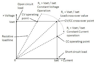
In most of our discussions in “Watt’s Up?” on current limiting we have primarily talked about power supplies as having a constant current (CC) output characteristic. This is what is found in many lab and industrial system power supplies, including most of the power supplies provided by us. Even though the terms often get used interchangeably, there is actually a distinction between constant current and current limit. To help explain this distinction, Figure 1 illustrates the output characteristics of a constant voltage/constant current (CV/CC) power supply.


Figure 1: Operating locus of a CC/CV power supply

Five operating points are depicted in Figure 1:
  1. With no load (i.e. infinite load resistance): Iout = 0 and Vout = Vset
  2. With a load resistance of RL > Vset/Iset: Iout = Vset/RL and Vout = Vset
  3. With a load resistance of RL = Vset/Iset: Iout = Iset and Vout = Vset
  4. With a load resistance of RL < Vset/Iset: Iout = Iset and Vout = Iset*RL
  5. With a short circuit (i.e. zero load resistance): Iout = Iset and Vout = 0


The advantage of a CV/CC power supply is it can be used as either a voltage source or a current source, providing reasonable performance in either mode. The point at which RL = Vset/Iset is the mode crossover point where the power supply transitions between CV and CC operation. For a CV/CC power supply there is a sharp transition between CV and CC operation. Note that for an ideal CV/CC power supply the CV slope is zero (horizontal), indicating zero output resistance for CV operation while the CC slope is infinite (vertical), indicating infinite output resistance for CC operation. Note that this is at DC. How close the slope of each mode is to ideal is what determines quality of load regulation for each.  To achieve good performance for both CV and CC modes requires carefully designed and more complex control loops for each mode. More details about using a power supply as a current source is provided in an earlier posting here, entitled: “Can a standard DC power supply be used as a current source?”

Constant Voltage/Current Limiting Power Supplies
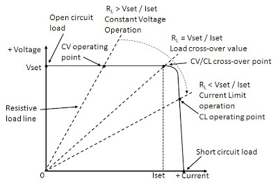
In comparison a constant voltage/current limiting (CV/CL) power supplies are intended to be used only as a voltage source while providing over-current protection for the DUT, as well as protection for the power supply itself. Figure 2 depicts typical output characteristics of a CV/CL power supply.


Figure 2: Operating locus of a CV/CL power supply

In CV/CL power supplies the current limit may be a fixed maximum value or it may be settable. In comparison to Figure 1 CV operation is still the same. However, what is found at the current limit cross-over point there is loss of voltage regulation where the voltage starts falling off. Unlike true CC operation in a CV/CC power supply, CL operation does not typically have as sharply a defined cross-over point and once in CL it may not be tightly regulated between the cross-over and short circuit points. The reason for this is CL control circuits are usually more basic in nature in comparison to a true CC control loop. CL is meant for over-current protection only, not CC operation.  For this reason the correct use of CL is to set its value a bit higher than the maximum current required by the DUT. This assures good voltage regulation for the full range of normal loading. You may find many of the more basic bench power supplies have CV/CL operation and may not be useful as current sources as a result.

Reference: Agilent Technologies DC Power Supply Handbook, application note AN-90B, part number 5952-4020

Monday, December 10, 2012

More on power supply current source-to-sink crossover characteristics


On my earlier posting “Power supply current source-to-sink crossover characteristics” I showed what the effects on the output voltage of a unipolar two-quadrant-power supply were, resulting from the output current on the power supply transitioning between sourcing and sinking. In that example scenario, the power supply was maintaining a constant output voltage and the transitioning between sourcing and sinking current was dictated by the external device connected to and being powered by the power supply. This is perhaps the most common scenario one will encounter that will drive the power supply between sourcing current and sinking current.

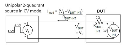
Other scenarios do exist that will drive a unipolar two-quadrant power supply to transition between sourcing and sinking output current. One scenario is nearly identical to the earlier posting. However, instead of the device transitioning its voltage between being less and greater than the power supply powering it, the power supply instead transitions its voltage between being less and greater than the active device being normally powered.  A set up for evaluating this scenario on an Agilent N6781A two-quadrant DC source is depicted in Figure 1.


Figure 1: Evaluating current source-to-sink crossover on an N6781A operating in constant voltage

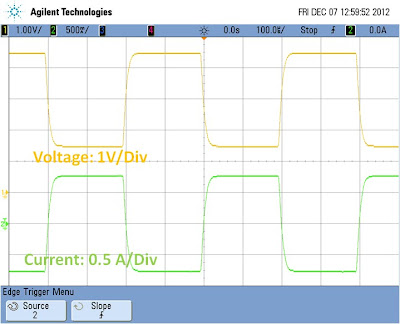
In this scenario having the DC source operating as a voltage source and transitioning between 1.5 and 4.5 volts causes the current to transition between -0.75 and +0.75A.  The voltage and current waveforms captured on an oscilloscope are shown in Figure 2.


Figure 2: Voltage and current waveforms for the set up in Figure 1

The waveforms in Figure 2 are as what should be expected. The actual transition points are where the current waveform passes through zero on the rising and falling edge. An expanded view to the current source-to-sink transition is shown in Figure 3.


Figure 3: Expanded voltage and current waveforms for the set up in Figure 1

As can be seen the voltage ramp transitions smoothly at the threshold point, or zero crossing point, of the current waveform. The reason being is that the DC is maintaining its operation as a voltage source. Its voltage feedback loop is always in control.


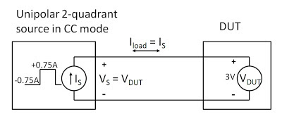
Yet one more scenario that will drive a unipolar two-quadrant source to transition between sourcing and sinking current is operate it as a current source and program is current setting between positive and negative values. In this case the device under test that was used is a voltage source.  One real-world example is cycling a rechargeable battery by alternately applying charging and discharging currents to it. The set up for evaluating this scenario, again using an N6781A two-quadrant DC source is depicted in Figure 4.


Figure 4: Evaluating current source-to-sink crossover on an N6781A operating in constant current

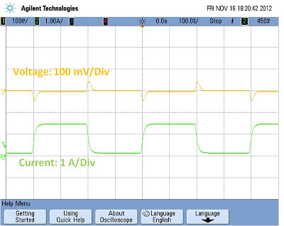
For Figure 4 the N6781A was set to operate in constant current and programmed to alternately transition between -0.75A and +0.75A current settings. The resulting voltage and current waveforms are shown in Figure 5.


Figure 5: Voltage and current waveforms for the set up in Figure 4

The waveforms in Figure 5 are as what should be expected. The actual transition points are where the current waveform passes through zero on the rising and falling edge. An expanded view to the current source-to-sink transition is shown in Figure 6.


Figure 6: Expanded voltage and current waveforms for the set up in Figure 4

As the N6781A is operating in current priority the interest is in how well it controls its current while transitioning through the zero-crossing point. As observed in Figure 6 it transitions smoothly through the zero-crossing point. The voltage performance is determined by the DUT, not the N6781A, as the N6781A is operating in constant current.

So what was found here is, for a unipolar two-quadrant DC source, transitioning between sourcing and sinking current should generally be virtually seamless as, under normal circumstances, should remain in either constant voltage or constant current during the entire transition.

Wednesday, December 5, 2012

Power supply current source-to-sink crossover characteristics


A two-quadrant power supply is traditionally one that outputs unipolar voltage but is able to both source as well as sink current. For a positive polarity power source, when sourcing current it is operating in quadrant 1 as a conventional power source. When sinking current it is operating in quadrant 2 as an electronic load. Conversely, a negative polarity two-quadrant  power source operates in quadrants three and four. Further details on power supply operating quadrants are provided in a recent posting here in ‘Watt’s Up?”, What is a bipolar (four-quadrant) power supply? Often a number of questions come up when explaining two-quadrant power supply operation, including:
  • What does it take to get the power supply operating as a voltage source to cross over from sourcing to sinking current?
  • What effect does crossing over from sourcing to sinking current have on the power supply’s output?


For a two-quadrant voltage source to be able to operate in the second quadrant as an electronic load, the device it is normally powering must also be able to source current and power as well as normally draw current and power. Such an arrangement is depicted in Figure 1, where the device is normally a load, represented by a resistance, but also has a charging circuit, represented by a switch and a voltage source with current-limiting series resistance.


Figure 1: Voltage source and example load device arrangement for two-quadrant operation.

There is no particular control on a two-quadrant power supply that one has to change to get it to transition from sourcing current and power to sinking current and power from the device it is normally powering. It is simply when the source voltage is greater than the device’s voltage then the voltage source will be operating in quadrant one sourcing power and when the source voltage is less than the device’s voltage the voltage source will be operating in quadrant two as an electronic load. In figure 1, during charging the load device can source current back out of its input power terminals as long as the charger’s current-limited voltage is greater than the source voltage.

It is assumed that load device’s load and charge currents are lower than the positive and negative current limits of the voltage source so that the voltage source always remains in constant voltage (CV) operation. A step change in current is the most demanding from a transient standpoint, but as the voltage source is always in its constant voltage mode it handle the transition well as its voltage control amplifier is always in control. This is in stark contrast to a mode cross over between voltage and current where different control amplifiers need to exchange control of the power supply’s output. In this later case there can be a large transient while changing modes. See another posting, Why Does My Power Supply Overshoot at Current Limit? Insights on Mode Crossover” for further information on this.  There is a specification given on voltage sources which quantifies the impact one should expect to see from a step change in current going from sourcing current to sinking current, which is its transient voltage response.  A transient voltage response measurement was taken on an N6781A two-quadrant DC source, stepping the load from 0.1 amps to 1.5 amps, roughly 50% of its rated output current.


Figure 2: Agilent N6781A transient voltage response measurement for 0.1A to 1.5A load step

However, the transient voltage response shown in Figure 2 was just for sourcing current. With a well-designed two-quadrant voltage source the transient voltage response should be virtually unchanged for any step change in current load, as long as it falls within the voltage source’s current range.  The transient voltage response for an N6781A was again capture in Figure 3, but now for stepping the load between -0.7A and +0.7A.


Figure 3: Agilent N6781A transient voltage response measurement for -0.7A to +0.7A load step

As can be seen in Figures 2 and 3 the voltage transient response for the N6781A remained unchanged regardless of whether the stepped load current was all positive or swung between positive and negative (sourcing and sinking).

While the transient voltage response addresses the dynamic current loading on the voltage source there is another specification that addresses the static current loading characteristic, which is the DC load regulation or load effect.  This is a very small effect on the order of 0.01% output change for many voltage sources. For example, for the N6781A the load effect in its 6 volt range is 400 microvolts for any load change. In the case of the N6781A being tested here the DC change was the same for both the 0.1 to 1.5 amp step and the -0.7 to +0.7 amp step change.


There are two more scenarios which will cause a two-quadrant power supply transition between current sourcing and sinking.  The first is very similar to above with the two-quadrant power supply operating in constant voltage (CV) mode, but instead of the DUT changing, the power supply changes its voltage level instead.  The final scenario is having the two-quadrant power supply operating in constant current with the DUT being a suitable voltage source that is able to source and sink power as well, like a battery for example. Here the two-quadrant power supply can be programmed to change from a positive current setting to a negative current setting, thus transitioning between sourcing and sinking current again, and its current regulating performance is now a consideration.  Both good topics for future postings!

Thursday, November 8, 2012

Configuring an Electronic Load for Zero Volt Operation


DC electronic loads are indispensable for testing a variety of DC power sources. There are a number of situations that call for testing DC power sources at low voltage, even right down to zero volts. Often this is also at relatively high current of many tens of amps or greater. Some examples include:
  • Low output voltage power supplies and DC/DC converters (mostly for digital circuit power)
  • Solar cell I-V testing, down to zero volts
  • Fuel cell testing
  • Single cell battery testing
  • Power supply true output short-circuit testing, down to zero volts


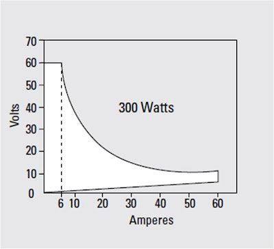
It becomes challenging for the test engineer to find adequate DC electronic loads for low voltage operation, especially at high currents. Many DC electronic loads, including the ones Agilent Technologies provides, use multiple power FETs for their input loading element. While a power FET can actually operate down to zero volts, this is at zero current as well. At high current a few volts is typically needed for stable, dynamic operation at full current.  As one example Figure 1 depicts the input I-V characteristics of an Agilent N3304A DC electronic load.


Figure 1: Agilent N3304A DC electronic load input I-V characteristics

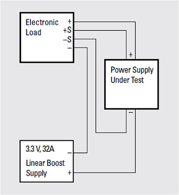
An effective solution for low voltage electronic load operation, right down to zero volts, for the electronic load’s full rated current, is to connect a low voltage boost power supply in series with the electronic load’s input. An example of this set up is depicted in Figure 2.


Figure 2: Zero volt DC electronic load set up

The electronic load now sees the sum of the boost supply’s and DUT’s voltages. Selecting a boost supply having adequate voltage will assure the electronic load will be able to operate at full performance at full current, even when the voltage at the DUT is zero. There are a few things that need to be paid attention to:
  • The electronic load needs to dissipate the total power of both the boost supply and DUT
  • The DUT needs to be adequately safeguarded against reverse polarity if the electronic load is inadvertently turned on too hard
  • The electronic load’s voltage sensing must be able to accommodate the extra voltage difference between the electronic load and DUT, due to the boost supply voltage
  • The boost supply ripple and noise (PARD) can contribute to noise measurements made on the DUT


Due to these considerations not all electronic loads may be well suited for zero volt operation with a boost supply so it is necessary to validate if a particular electronic load under consideration can be applied in this manner first.  Further details about zero voltage load operation as well as using Agilent N3300 series DC electronic loads for this purpose are described in product note “Agilent Zero Volt Electronic Load”, publication number 5968-6360E. Click here to access

Tuesday, July 17, 2012

How Does a Power Supply regulate It’s Output Voltage and Current?


We have talked about Constant Voltage (CV) and Constant Current (CC) power supply operation in many various ways and applications here on the “Watt’s Up?” blog in the past. Indeed, CV and CC are fundamental operating modes of most all power supplies. But what exactly takes place inside the power supply that endows it with the ability to regulate either its output voltage or current, depending on the load? If you ever wondered about this, wonder no longer!

Most all power supplies regulate either their output voltage or output current at a constant level, depending on the load resistance relative to the power supply’s output voltage and current settings. This can be summarized as follows:

·         If R load > (V out / I out) then power supply is in CV mode
·         If R load < (V out / I out) then power supply is in CC mode

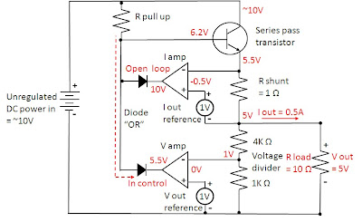
To accomplish this most all power supplies have separate voltage and current feedback control loops to limit either the output voltage or current, depending on the load. To illustrate this Figure 1 shows a circuit diagram of a basic 5 volt, 1 amp output series regulated power supply operating in CV mode.


Figure 1: Basic DC Power Supply Circuit, Constant Voltage (CV) Operation

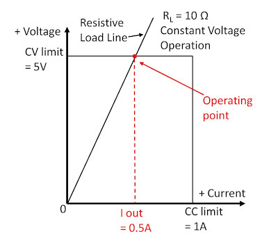
The CV and CC control loops/amplifiers each have a reference input value. In this case the reference values are both 1 volt. In order to regulate output voltage the CV error amplifier compares its 1 volt reference against a resistor divider that divides the output voltage down by a factor of 5, limiting the output voltage to 5 volts. Likewise the CC error amplifier compares its 1 volt reference against a 1 ohm current shunt resistor located in the output current path, limiting the output current to 1 amp. For Figure 1 the load resistance is 10 ohms. Because this load resistance is greater than (V out / I out) = 5 ohms, the power supply is operating in CV mode. The CV error amplifier takes control of the series pass transistor by drawing away excess base current from the series pass transistor, though the diode “OR” network. The CV amplifier is operating in closed loop, maintaining its error voltage at zero volts. In comparison, because the actual output current is only 0.5 amps the CC amplifier tries to turn the current on harder but cannot because the CV amplifier has control of the output. The CC amplifier is operating open loop. Its output goes up to its positive limit while it has -0.5 volts of error voltage. The output I-V diagram for this Constant Voltage operation is shown in Figure 2.


Figure 2: Power Supply I-V Diagram, CV Operation

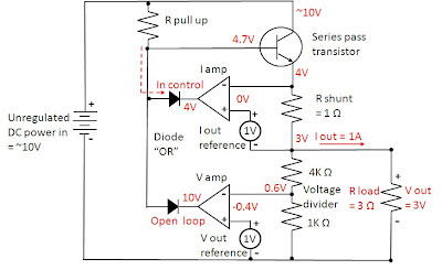
Now say we increase the load by lowering the output load resistance from 10 ohms down to 3 ohms. Figure 3 shows the circuit diagram of our basic 5 volt, 1 amp output series regulated power supply revised for operating in CC mode with a 3 ohm load resistor.


Figure 3: Basic DC Power Supply Circuit, Constant Current (CC) Operation

Because the load resistor is lower than (V out / I out) = 5 ohms, the power supply switches to CC mode. The CC error amplifier takes control when the voltage drop on the current shunt resistor increases to match the 1 volt reference value, corresponding to 1 amp output, drawing excess base current from the series pass transistor though the diode “OR” network. The CC amplifier is now operating closed loop, regulating the output current to maintain its input error voltage at zero. In comparison, because the actual output voltage is now only 3 volts the CV amplifier tries to increase the output voltage but cannot because the CC amplifier has control of the output. The CV amplifier is operating open loop. Its output now goes up to its positive limit while it has -0.4 volts of error voltage. The output I-V diagram for this Constant Current operation is shown in Figure 4.


Figure 4: Power Supply I-V Diagram, CC Operation

As we have seen most all power supplies have separate current and voltage control loops to regulate their outputs in either a Constant Voltage (CV) or in a Constant Current (CC) mode. One or the other takes control, depending on that the load resistance is in relation to what the power supply’s output voltage and current settings are. In this way both the load and power supply are protected by limiting the voltage and current that is delivered by the power supply to the load. By understanding this theory behind a power supply’s CV and CC operation it is also easier to understand the underlying reason for why various power supply characteristics are the way they are, as well as see how other power supply capabilities can be created by building on top of this foundation. Stay tuned!

Wednesday, September 21, 2011

What is load effect and how does it affect my testing?

Load effect is a power supply specification (also known as load regulation) that describes how well the power supply can maintain its steady-state output setting when the load changes. More formally, it specifies the maximum change in steady-state DC output voltage (or current) resulting from a specified change in the load current (or voltage), with all other influence quantities maintained constant. So, when a power supply is regulating its output voltage in CV (constant voltage) mode, this specification tells you how much the voltage can change when the current changes. Here is an example:

Let’s say the voltage load effect specification for a 20 V, 5 A power supply is 2 mV and is specified for any load change. This means for any current change within the rating of the supply (in this case, up to 5 A), the output voltage will not change by more than 2 mV. For example, if the power supply is set to 10 V, the actual output may measure 9.999 V with no load (0 A). (Note that the difference between the setting and the actual output voltage is a different specification called programming accuracy.) If you then increase the current from 0 A to a full load condition of 5 A, the load effect specification guarantees that the output voltage will not change by more than 2 mV, so it will be somewhere between 9.997 V and 10.001 V. So if the actual output voltage started at 9.999 V with a 0 A load and measured 9.9982 V with a 5 A load, the load effect for this output when set for 10 V measures 0.8 mV (9.999 – 9.9982), well within the 2 mV specification. You must make the second voltage measurement immediately following the load current change to avoid capturing any short-term drift effects.


In the above example, the specified change in load current was “any load change”. Of course, it is implied that the load change is within the output ratings of the supply. You cannot change the output current from 0 A to 100 A on a 5 A power supply. Some load effect specifications state that the load change is a 50% change (e.g., 2.5 A to 5 A) while others may say 10% to 90% of full load (e.g., 0.5 A to 4.5 A).

And what does “with all other influence quantities maintained constant” mean? Things like temperature and the AC line input voltage can affect the output parameter, so these things must be held constant in order to see only the effect of the load change. The effects on the power supply output of changes in each of these influencing quantities (temperature, AC line input voltage) are described in different specifications.

Most performance power supplies have load effect specifications in the range of just a few hundred uV up to a few mV. A lower performance model may have a load effect specification of between 10 mV and 100 mV. Power supplies with higher maximum voltage ratings and higher maximum power ratings typically have higher load effect specifications.

If you have an application where maintaining an exact voltage at your DUT is critical and your DUT draws different amounts of current at different times, you will want to use a power supply with a low load effect specification. If changes in the voltage at your DUT with changes in DUT current are less critical to you, most power supplies will perform well for your application.