Showing posts with label over voltage protect. Show all posts

Tuesday, November 18, 2014

Why does the response time of OCP vary on the power supply I am using and what can I do about it? Part 1

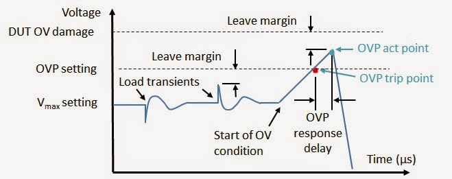
In a previous posting of mine “Providing effective protection of your DUT against over voltage damage during test”(click here to review), an important consideration for effective protection was to factor in the response time of the over voltage protect (OVP) system. Due to the nature of over voltage damage, the OVP must be reasonably fast. The response time can typically be just a few tens of microseconds for a reasonably fast OVP system on a higher performance system power supply to hundreds of microseconds on a more basic performance system power supply. This response time usually does not vary greatly with the amount of over voltage being experienced.

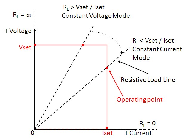
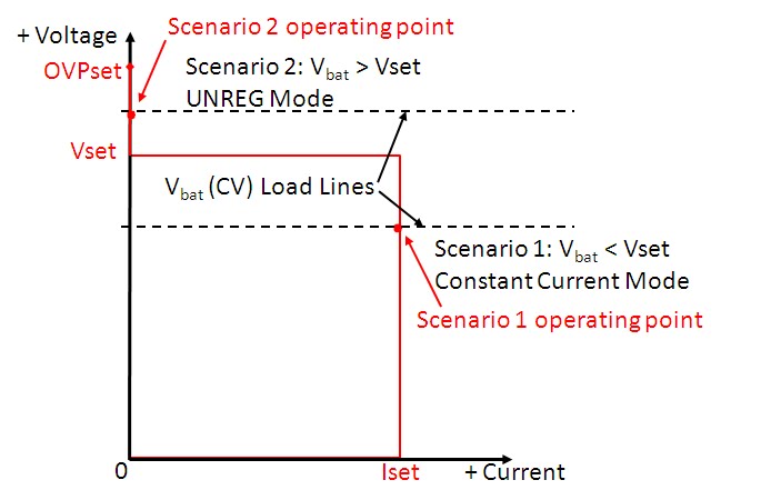
Just as with voltage, system power supplies usually incorporate over current protect (OCP) systems as well. But unlike over voltage damage, which is almost instantaneous once that threshold is reached, over current takes more time to cause damage. It also varies in some proportion to the current level; lower currents taking a lot longer to cause damage. The I2t rating of an electrical fuse is one example that illustrates this effect.

Correspondingly, like OVP, power supply OCP systems also have a response time. And also like OVP, the test engineer needs to take this response time into consideration for effective protection of the DUT.  However, unlike OVP, the response time of an OCP system is quite a bit different. The response time of an OCP system is illustrated in Figure 1.


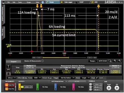
Figure 1: Example OCP system response time vs. overdrive level

Here in Figure 1 the response time of the OCP system of a Keysight N7951A 20V, 50A power supply was characterized using the companion 14585A software. It compares response times of 6A and 12A loading when the current limit is set to 5A. Including the programmed OCP delay time of 5 milliseconds it was found that the actual total response time was 7 milliseconds for 12A loading and 113 milliseconds for 6A loading.

This is quite different than the response time of an OVP system. Even if the OCP delay time was set to zero, the response is still on the order of milliseconds instead of microseconds for the OVP system. And when the amount of overdrive is small, as is the case for the 6A loading, providing just 1A of overdrive, the total response time is much greater. Why is that?

Unlike the OVP system, which operates totally independent of the voltage limit control system, the OCP system is triggered off the current limit control system. Thus the total response time includes the response time of the current limit as well. The behavior of a current limit is quite different than a simple “go/no go” threshold detector as well. A limit system, or circuit, needs to regulate the power supply’s output at a certain level, making it a feedback control system. Because of this stability of this system is important, both with crossing over from constant voltage operation as well as maintaining a stable output current after crossing over. This leads to the slower and overdrive dependent response characteristics that are typical of current limit systems.

So what can be done about the slower response of an OCP system? Well, early on in this posting I talked about the nature of over current damage. Generally over current damage is much slower by nature and the over drive dependent response time is in keeping with time dependent nature of over current damage. The important thing is understand what the OCP response characteristic is like and what amount of over current your DUT is able to sustain, and you should be able to make effective use of the over current protection capabilities of your system power supply.

If however you are still looking how you might further improve on OCP response speed, look for my follow up to this in my next posting!

Friday, November 7, 2014

Providing effective protection of your DUT against over voltage damage during test

The two most common ways DUTs can be electrically damaged during test are from current-related events or voltage-related events that mange to over-stress the DUT. Sometimes the cause can be an issue with the DUT itself. Other times it can be an issue stemming from the test system. The most common voltage-related damage to a DUT is an over voltage event, beyond a maximum level the DUT can safely tolerate. While there are a number of things that can cause this, most invariably it was an issue with the test system power supply, either from inadvertently being set too high or from an internal failure.

To protect against accidental over voltage damage, test system power supplies incorporate an over voltage protect (OVP) system that quickly shuts down the output upon detecting the voltage has gone above a preset threshold value. More details about OVP have been written about here in a previous posting “Overvoltage protection: some background and history”(click here to review).

The critical thing about over voltage damage is, in most all cases, that it is virtually immediate once the voltage threshold where damage to the DUT occurs is exceeded. It is therefore imperative that you optimize the test set up and settings in order to provide effective protection of your DUT against over voltage damage during test. To start with, the OVP trip threshold needs to be set at a reasonable amount below the threshold where DUT damage occurs and at the same time be set to a reasonable amount above the maximum expected DUT operating voltage. This is depicted in Figure 1.


Figure 1: OVP set point

However, to understand what are “reasonable amounts” above the maximum operating voltage and below the DUT damage voltage levels you need to take into account the dynamic response characteristics of the power supply output and OVP system, as depicted in Figure 2.


Figure 2: Power supply output and OVP dynamic response characteristics

It is important to have adequate margin above the maximum operating voltage to account for transient voltages due to the DUT drawing current from the power supply and resulting voltage response of the power supply in correcting for this loading, in order to prevent false OVP tripping. It is likewise important to adequate margin below the DUT damage threshold as it takes a small amount of time, in the range of 10’s to 100’s of microseconds, for the OVP system to start shutting down the power supply’s output once the OVP trip point has been crossed. At the same time the power supply typically has a maximum rate the output voltage can slew in. In practice these “reasonable amounts” typically need to be a few tenths to several tenths of a volt as a minimum.

Generally these margins are not difficult to manage, except when the DUT’s operating voltage is very small or the DUT operating current is very large producing a correspondingly large voltage drop in the power supply wiring. This is because the OVP is traditionally sensed on power supply’s output power terminals, so that it provides protection regardless of what the status and condition of the remote voltage sense wiring connection is. To improve on this we also provide OVP sensing on the remote sensing wires as an alternative to, or in addition to, the traditional sensing on the output power terminals. More details about this are described in another posting here “Protect your DUT: Use sense leads for over voltage protection (OVP)”(click here to review).

By following these suggestions you should be able to effectively protect your DUT against over voltage damage during test as well!

Tuesday, August 5, 2014

Upcoming Seminar on Protecting Your Device against Power-Related Damage during Test

Here on “Watt’s Up?” we have provided a good number of posts about various protection features incorporated into system power supplies to protect your device against power-related damage during test. Just recently my colleague Gary posted “How Does Power Supply Over-Voltage Work?” (Click here to review) Here he reviews inner workings of different OVP implementations.  I recently posted “Safeguarding Your Power-Sensitive DUTs against an Over-Power Condition” (Click here to review) Here I go over a method to protect your DUT against excess power when other power supply features like over current protection may be less than ideal.

The reason why we frequently share power-related protection topics here is protecting your DUT is extremely important, there are a lot of different capabilities incorporated in system power supplies for this purpose, and there are a lot of practical considerations when putting them to use.  

Hopefully a number of you have found our posts on protection-related topics of help. Because this is a very important topic and there is so much more you should know about it I will be giving a live web-based seminar “Protecting Your Device against Power-Related Damage during Test” on August 20th, just a few weeks away from today. I will be going over a number of protection-related topics which we have not yet covered here on “Watt’s Up?”.  One of my objectives is to provide a more holistic view of the many ways a system power supply is able to better safeguard against power-related damage as well as what is practical to expect when using these various capabilities incorporated in the power supply.

You can register online at the following (Click here for description and registration page) In case you are not able to attend the live event on August 20 you will be able to register and listen to seminar afterward as well, as it will be recorded.


So if protecting your device against power-related damage is important to you I hope you are able to attend the seminar!

Monday, June 23, 2014

Safeguarding your power-sensitive DUTs from an over power condition

Today’s system DC power supplies incorporate quite a variety of features to protect both the device under test (DUT) as well as the power supply itself from damage due to a fault condition or setting mishap. Over voltage protect (OVP) and over current protect (OCP) are two core protection features that are found on most all system DC power supplies to help protect against power-related damage.

OVP helps assure the DUT is protected against power-related damage in the event voltage rises above an acceptable range of operation. As over voltage damage is almost instantaneous the OVP level is set at reasonable margin below this level to be effective, yet is suitably higher than maximum expected DUT operating voltage so that any transient voltages do not cause false tripping. Causes of OV conditions are often external to the DUT.

OCP helps assure the DUT is protected against power-related damage in the event it fails in some fashion causing excess current, such as an internal short or some other type of failure. The DUT can also draw excess current from consuming excess power due to overloading or internal problem causing inefficient operation and excessive internal power dissipation.

OVP and OCP are depicted in Figure 1 below for an example DUT that operates at a set voltage level of 48V, within a few percent, and uses about 450W of power. In this case the OVP and OCP levels are set at about 10% higher to safeguard the DUT.


Figure 1: OVP and OCP settings to safeguard an example DUT

However, not all DUTs operate over as limited a range as depicted in Figure 1. Consider for example many, if not most all DC to DC converters operate over a wide range of voltage while using relatively constant power. Similarly many devices incorporate DC to DC converters to give them an extended range of input voltage operation. To illustrate with an example, consider a DC to DC converter that operates from 24 to 48 volts and runs at 225W is shown in Figure 2. DC to DC converters operate very efficiency so they dissipate a small amount of power and the rest is transferred to the load. If there is a problem with the DC to DC converter causing it to run inefficiently it could be quickly damaged due to overheating. While the fixed OCP level depicted here will also adequately protect it for over power at 24 volts, as can be seen it does not work well to protect the DUT for over power at higher voltage levels.


Figure 2: Example DC to DC converter input V and I operating range

A preferable alternative would instead be to have an over power protection limit, as depicted in Figure 3. This would provide an adequate safeguard regardless of input voltage setting.


Figure 3: Example DC to DC converter input V and I operating range with over power protect

As an over power level setting is not a feature that is commonly found in system DC power supplies, this would then mean having to change the OCP level for each voltage setting change, which may not be convenient or desirable, or in some cases practical to do. However, in the Agilent N6900A and N7900A Advance Power System DC power supplies it is possible to continually sense the output power level in the configurable smart triggering system. This can in turn be used to create a logical expression to use the output power level to trigger an output protect shutdown. This is depicted in Figure 4, using the N7906A software utility to graphically configure this logical expression and then download it into the Advance Power System DC power supply. As the smart triggering system operates at hardware speeds within the instrument it is fast-responding, an important consideration for implementing protection mechanisms.


Figure 4: N7906A Software utility graphically configuring an over power protect shutdown

A glitch delay was also added to prevent false triggers due to temporary peaks of power being drawn by the DUT during transient events. While the output power level is being used here to trigger a fault shutdown it could have been just as easily used to trigger a variety of other actions as well.

Thursday, April 3, 2014

Why have programmable series resistance on a power supply’s output?

A feature we’ve included on our 663xxA Mobile Communications DC Sources, our N6781A 2-quadrant Source Measure Module, and most recently our N69xxA and N79xxA Advanced Power System (APS) is the ability to program in a value for a resistance that exists in series with the output voltage. So why do we offer this?

 Batteries are not ideal voltage sources. They have a significant amount of equivalent series resistance (ESR) on their output. Because of this, the battery’s output has a voltage drop that is proportional to the current drawn by the DUT that is being powered. An example of this is shown in the oscilloscope capture in Figure 1, where a GPRS mobile handset is drawing pulsed transmit current from its battery.


Figure 1: Battery voltage and current powering a GPRS handset during transmit

In comparison, due to control feedback, a conventional DC power supply has extremely low output impedance. At and near DC, for all practical purposes, the DC output resistance is zero. At the same time, during fast load current transition edges, many conventional DC power supplies can have fairly slow transient voltage response, leading to significant transient overshoots and undershoots with slow recovery during these transitions, as can be seen in the oscilloscope capture in Figure 2.


Figure 2: Example general purpose bench power supply powering a GPRS handset during transmit

It’s not hard to see that the general purpose bench power supply voltage response is nothing close to that of the battery’s voltage response and recognize that it will likely have a significant impact on the performance of the GPRS handset. Just considering the performance of the battery management, the battery voltage drop during loading and rise during charging, due to the battery’s resistance, will impact discharge and charge management performance.

We include programmable resistance in the above mentioned DC power supplies as they are battery simulators.  By being able to program a series output resistance these power supplies are able to better simulate the voltage response of a battery, as shown in Figure 3.


Figure 3: N6781A battery simulator DC source powering a GPRS handset during transmit

While the 663xxA and N6781A are fairly low power meant to simulate batteries for handheld mobile devices, The N69xxA and N79xxA APS units are 1 and 2 KW power supplies meant to simulate much larger batteries used in things like satellites, robotics, regenerative energy systems, and a number of other higher power devices. Figure 4 shows the voltage response of an N7951A 1 KW APS unit programmed to 20 milliohms output impedance, having a +/- 10 amp peak sine wave load current applied to its output.


Figure 4: N7951A 1 KW APS DC source voltage response to sine wave load

Programmable series output resistance is one more way a specialized DC source helps improve performance and test results, in this case doing a better job simulating the battery that ultimately powers the device under test.

Tuesday, March 12, 2013

What is a power supply’s over current protect (OCP) and how does it work?


One feature we include in our Agilent system DC power supplies for providing additional safeguard for overload-sensitive DUTs is over current protect, or OCP. While some may think this is something separate and independent of current limiting, OCP actually works in concert with current limiting.

Current limiting protects overload-sensitive DUTs by limiting the maximum current that can be drawn by the DUT to a safe level. There are actually a variety of current limit schemes, depending on the level of protection required to safeguard the DUT during overload. Often the current limit is relatively constant, but sometimes it is not, depending on what is best suited for the particular DUT. Additional insights on current limits are provided in an earlier posting, entitled “Types of current limits for over-current protection on DC power supplies“.

By limiting the current to a set level may DUTs are adequately protect from too much current and potential damage. When in current limit, if the overload goes away the power supply automatically goes back to constant voltage (CV) operation. However, current limit may not be quite enough for some DUTs that are very sensitive to overloads. This is where OCP works together with the current limit to provide an additional level of protection. With OCP turned on, when the DC power supply enters into current limit OCP takes over after a specified time delay and shuts down the output of the DC power supply. The delay time is programmable. This prevents OCP from shutting down the DC power supply from short current spikes and other acceptably short overloads that are not considered harmful. Like over voltage protect or OVP, after tripping the output needs to be disabled and an Output Protect Clear needs to be exercised in order to reset the power supply so that its output can be re-enabled.  Unlike OVP, OCP can be turned on and off and its default is usually off. In comparison, OVP is usually always enabled and cannot be turned off. A typical OCP event is illustrated in Figure 1.


Figure 1: OCP operation

When powering DUTs, either on the bench or in a production test system, it is always imperative that adequate safeguards are taken to protect both the DUT as well as the test equipment from inadvertent damage. Over current protect or OCP is yet another of many features incorporated in system DC power supplies you can take advantage of to protect overload-sensitive DUTs from damage during test!

Friday, February 15, 2013

Addressing the challenge of sequencing multiple bias supplies on and off


A challenge test engineers are perennially faced with is how to best sequence the bias voltages powering their DUT, when their DUT requires several bias voltages. Many DUTs are sensitive to sequencing and an improper sequence may lead to the DUT hanging up, or worse, suffer damage as a consequence. Not only is sequencing an issue when powering the DUT on, but it can also be an issue when powering the DUT down as well. In addition to sequencing, the slew rates of the various bias voltages can likewise be important to the DUT correctly powering on.

Simply relying on the timing of output-on and output-off commands sent from the test system controller to all the system DC power supplies individually tends to be far too imprecise, especially for critical sequencing timing requirements. The actual turn-on time of a typical system DC power supply can be many tens of milliseconds, and will vary considerably between different models of power supplies. The turn-on and turn-off times of each will need to be carefully characterized in order to know when a command for a specific bias voltage needs to be sent in relation to the other bias voltages. It is very likely the sequence of commands sent for outputs to turn on or off may be in a different sequence to the outputs actually changing, due to delay differences between different DC power supplies! An even bigger problem however is most system controllers are PCs which may randomly experience a large delay in sending out a command, if a higher level service request interrupts and pre-empts execution of the test program.

An alternative approach often taken is adding some custom hardware to control output sequencing. This can assure correct sequencing, but adds a lot of complexity, is usually inflexible, and may introduce other issues and compromises.

At Agilent we added system features to our N6700 series multiple output modular DC power system that support correct power-on and power-off sequencing. The output-on and output-off controls for the individual outputs get grouped together. The N6700 platform knows and compensates for the actual delays of all the various DC power output modules so that the desired delay value entered will be what is accurately achieved. Figure 1 shows setting up an N6705A to achieve a desired turn-on sequence of DC outputs for powering up a PC mother board. Figure 2 shows the actual result. A more detailed description of this PC motherboard example is given in our application note: “Biasing Multiple Input Voltage Devices in R&D”. While the N6705B DC Power Analyzer mainframe is regarded as being primarily for R&D, which this app note is referencing, the low profile rack-mountable N6700 series mainframes have these very same features and suit automated test systems in manufacturing and other environments.


Figure 1: Setting Output Delays


Figure 2: Output Turn-on Sequence Results


Just like setting up the power-on sequence, separate delays for power-off can also be entered, as seen in the set up screen shown in Figure 1, for the expected shut down of the DUT. However, what if there is an emergency shut down due to an abnormal condition and you still want to assure a certain power-off sequence? A colleague worked out the procedure for setting up the N6700 series DC power system to provide an orderly shutdown of the outputs, in the event of a problem on one of the outputs. In this example it happens to be an overvoltage condition on one of the outputs, but any of a number of fault conditions can be acted on to initiate an orderly shutdown. Details of this procedure are provided in another application note; “Avoid DUT Damage by Sequencing Multiple Power Inputs Off Upon a Fault Event”.

So when faced with the challenge of having to properly sequence multiple DC bias voltages powering your DUT, reconsider trying to engineer a solution to accomplish this. Instead, look for features that provide this kind of capability in the system DC power supplies you are looking to use, already built-in. It makes a lot of sense having sequencing built into the power supplies and it will make your life a lot easier!

Friday, February 8, 2013

Protecting your DUT using a power supply’s remote inhibit and fault indicator features


Paramount in most any good electronic test system is the need to adequately protect the device under test (DUT), as well as the test equipment, from inadvertent damage due to possible faults with the yet-untested DUT, accidental misconnections, misapplication of power, and a large number of other unanticipated events that can occur. It is no surprise that a lot of these unanticipated events by nature are related to the powering of the DUT. For this reason good system DC power supplies incorporate a number of features designed to protect both the DUT, as well as the power supply, in the event of an unanticipated fault occurring.  Two related protection features incorporated into our DC system power supplies are the remote inhibit and the discrete fault indicator (RI/DFI). These features provide real-time protection enabling immediate shutting down the power supply, as well as enabling the power supply to take immediate action, on the event of detecting the occurrence of an unanticipated event or fault.

The remote inhibit is a digital input control while the discrete fault indicator is a digital output control signal, incorporated into the digital I/O port on our system DC power supplies. An example of a digital I/O port is illustrated in Figure 1. When the digital I/O port is configured for fault/inhibit (also called RI/DFI) pins 1 and 2 are the open collector and emitter of an isolated transistor, to serve as a digital output control, and pin3 and 4 are the digital input and common for the inhibit control input. The remote inhibit and the fault indicator can be used independently as well as in combination, for protecting the DUT.


Figure 1: Multi-function digital I/O port on Agilent 6600A series system DC power supplies

As the name implies, the remote inhibit is a digital control input, when activated, immediately disables the DC power supply’s output. One way this is commonly used is to connect an emergency shutdown switch that can be conveniently activated in the event of a problem. This may be a large pushbutton, or it may be a switch incorporated into a fixture safety cover. This arrangement is shown in Figure 2.


Figure 2: Remote inhibit using external switch

The fault indicator (i.e. FLT, FI, or DFI) digital output signal originates from the system DC power supply’s status system. The status system is a configurable logic system within the power supply having a number of registers that keep track of its status for operational, questionable, and standard events. Many of these events can be logically OR’ed together as needed to provide a fault output signal when particular, typically unanticipated, events occurs with the power supply. Items tracked by questionable status group register, like over voltage and over current, for example, are commonly selected and used for generating a fault output signal. An overview of the power supply status register system was discussed by a colleague in a previous posting. If you are interested in learning more; click here.
The fault indicator output can in turn be used to control an external activity for protecting the DUT, such as opening a disconnect relay to isolate the DUT, as one example, as depicted in Figure 3.


Figure 3: Fault output controlling an external disconnect relay

For DUTs that require multiple bias voltage inputs it is usually desirable that if a fault is detected on one bias input, that the other bias inputs are immediately shut down in conjunction with the one detecting a fault. The fault outputs and remote inhibit inputs on several DC power supplies can be used in combination by chaining them together, as depicted in Figure 4, to accomplish this task, to safeguard the DUT.


Figure 4: Chaining fault indicators and remote inhibits on multiple DC power supplies

The remote inhibit and fault indicator digital control signals on system DC power supplies provide a number of ways to disable power and take other actions for safeguarding the DUT. Their action is immediate, not requiring communication to, and intervention from, the test system controller. At the same time the system DC power supply generates status signals and can issue a service request (SRQ) to the test system controller so that it is notified of a problem condition and take appropriate correction action as well. The remote inhibit and fault indicator digital control signals are just two of many features found in many good system DC power supplies to assure the DUT is always adequately protected during test!

Wednesday, March 28, 2012

What Is Going On When My Power Supply Displays “UNR”?

Most everyone is familiar with the very traditional Constant Voltage (CV) and Constant Current (CC) operating modes incorporated in most any lab bench or system power supply. All but the most very basic power supplies provide display indicators or annunciators to indicate whether it is in CV or CC mode. However, moderately more sophisticated power supplies provide additional indicators or annunciators to provide increased insight and more information about their operating status. One annunciator you may encounter is seeing “UNR” flash on, either momentarily or continuously. It’s fairly obvious that this means that the power supply is unregulated; it is failing to maintain a Constant Voltage or Constant Current. But what is really going on when the power supply displays UNR and what things might cause this?
To gain better insight about CV, CC and UNR operating modes it is helpful to visualize what is going on with an IV graph of the power supply output in combination with the load line of the external device being powered. I wrote a two part post about voltage and current levels and limits which you may find useful to review. If you like you can access it from these links levels and limits part 1 and levels and limits part 2. This posting builds nicely on these earlier postings. A conventional single quadrant power supply IV graph with resistive load line is depicted in Figure 1. As the load resistance varies from infinity to zero the power supply’s output goes through the full range of CV mode through CC mode operation. With a passive load like a resistor you are unlikely to encounter UNREG mode, unless perhaps something goes wrong in the power supply itself.
Figure 1: Single quadrant power supply IV characteristic with a resistive load

However, with active load devices you have a pretty high chance of encountering UNR mode operation, depending where the actual voltage and current values end up at in comparison to the power supply’s voltage and current settings. One common application where UNR can be easily encountered is charging a battery (our external active load device) with a power supply. Two different scenarios are depicted in Figure 2. For scenario 1, when the battery voltage is less than the power supply’s output, the point where the power supply’s IV characteristic curve and the battery’s load line (a CV characteristic) intersect, the power supply is in CC mode, happily supplying a regulated charge current into the battery. However, for scenario 2 the battery’s voltage is greater than the power supply’s CV setting (for example, you have your automobile battery charger set to 6 volts when you connect it to a 12 volt battery). Providing the power supply is not able to sink current the battery forces the power supply’s output voltage up along the graph’s voltage axis to the battery’s voltage level. Operating along this whole range of voltage greater than the power supply’s output voltage setting puts the power supply into its UNR mode of operation.
Figure 2: Single quadrant power supply IV characteristic with a battery load

A danger here is more sophisticated power supplies usually incorporate Over Voltage Protection (OVP). One kind of OVP is a crowbar which is an SCR designed to short the output to quickly bring down the output voltage to protect the (possibly expensive) device being powered. When connected to a battery if an OVP crowbar is tripped, damage to the power supply or battery could occur due to batteries being able to deliver a fairly unlimited level of current. It is worth knowing what kind of OVP there is in a power supply before attempting to charge a battery with it. Better yet is to use a power supply or charger specifically designed to properly monitor and charge a given type of battery. The designers take these things into consideration so you don’t have to!
I have digressed here a little on yet another mode, OVP, but it’s all worth knowing when working with power supplies! Can you think of other scenarios that might drive a power supply into UNR? (Hint: How about the other end of the power supply IV characteristic, where it meets the horizontal current axis?)