A two-quadrant power supply is traditionally one that
outputs unipolar voltage but is able to both source as well as sink current.
For a positive polarity power source, when sourcing current it is operating in
quadrant 1 as a conventional power source. When sinking current it is operating
in quadrant 2 as an electronic load. Conversely, a negative polarity
two-quadrant power source operates in
quadrants three and four. Further details on power supply operating quadrants
are provided in a recent posting here in ‘Watt’s Up?”, “What is a bipolar (four-quadrant) power supply?”
Often a number of questions come up when explaining two-quadrant power supply
operation, including:
- What does it take to get the power supply operating as a voltage source to cross over from sourcing to sinking current?
- What effect does crossing over from sourcing to sinking current have on the power supply’s output?
For a two-quadrant voltage source to be able to operate in
the second quadrant as an electronic load, the device it is normally powering
must also be able to source current and power as well as normally draw current
and power. Such an arrangement is depicted in Figure 1, where the device is normally
a load, represented by a resistance, but also has a charging circuit,
represented by a switch and a voltage source with current-limiting series
resistance.
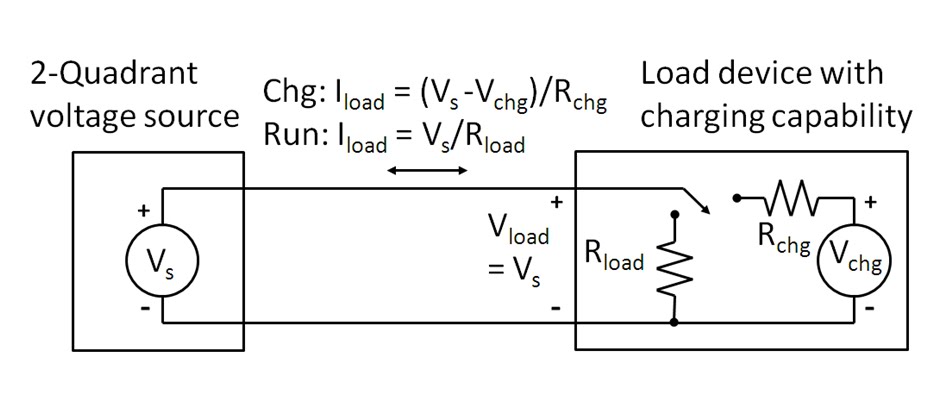
Figure 1: Voltage source and example load device
arrangement for two-quadrant operation.
There is no particular control on a two-quadrant power
supply that one has to change to get it to transition from sourcing current and
power to sinking current and power from the device it is normally powering. It
is simply when the source voltage is greater than the device’s voltage then the
voltage source will be operating in quadrant one sourcing power and when the
source voltage is less than the device’s voltage the voltage source will be
operating in quadrant two as an electronic load. In figure 1, during charging
the load device can source current back out of its input power terminals as long as the
charger’s current-limited voltage is greater than the source voltage.
It is assumed that load device’s load and charge currents
are lower than the positive and negative current limits of the voltage source
so that the voltage source always remains in constant voltage (CV) operation. A
step change in current is the most demanding from a transient standpoint, but as
the voltage source is always in its constant voltage mode it handle the
transition well as its voltage control amplifier is always in control. This is
in stark contrast to a mode cross over between voltage and current where
different control amplifiers need to exchange control of the power supply’s
output. In this later case there can be a large transient while changing modes.
See another posting, “Why Does My Power
Supply Overshoot at Current Limit? Insights on Mode Crossover” for further information on this. There is a specification given on voltage
sources which quantifies the impact one should expect to see from a step change
in current going from sourcing current to sinking current, which is its
transient voltage response. A transient
voltage response measurement was taken on an N6781A two-quadrant DC source,
stepping the load from 0.1 amps to 1.5 amps, roughly 50% of its rated output current.

Figure 2: Agilent N6781A transient voltage response
measurement for 0.1A to 1.5A load step
However, the transient voltage response shown in Figure 2
was just for sourcing current. With a well-designed two-quadrant voltage source
the transient voltage response should be virtually unchanged for any step
change in current load, as long as it falls within the voltage source’s current
range. The transient voltage response
for an N6781A was again capture in Figure 3, but now for stepping the load
between -0.7A and +0.7A.

Figure 3: Agilent N6781A transient voltage response
measurement for -0.7A to +0.7A load step
As can be seen in Figures 2 and 3 the voltage transient
response for the N6781A remained unchanged regardless of whether the stepped
load current was all positive or swung between positive and negative (sourcing
and sinking).
There are two more scenarios which will cause a
two-quadrant power supply transition between current sourcing and sinking. The first is very similar to above with the
two-quadrant power supply operating in constant voltage (CV) mode, but instead
of the DUT changing, the power supply changes its voltage level instead. The final scenario is having the two-quadrant
power supply operating in constant current with the DUT being a suitable
voltage source that is able to source and sink power as well, like a battery
for example. Here the two-quadrant power supply can be programmed to change
from a positive current setting to a negative current setting, thus
transitioning between sourcing and sinking current again, and its current
regulating performance is now a consideration.
Both good topics for future postings!