Friday, August 31, 2012

To autoscale, or not to autoscale: that is the question!

While the primary focus of this blog is power, this post is about a topic that applies beyond just power: autoscale. I want our readers to comment on this topic:

 Should a test equipment user use the autoscale button or not? If so, why? If not, why not?

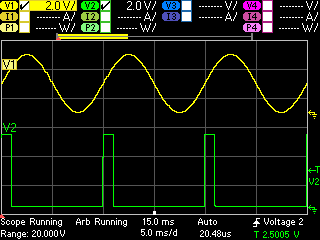
How is autoscale related to power, you ask? One of our Agilent power products, the N6705B DC Power Analyzer, has a build-in scope-like function with an autoscale button. The built-in scope is useful for measuring things like dynamic current flowing into a device or for looking at the response to an arbitrary waveform that can also be generated with the same product. To autoscale in Scope View mode, you push an N6705B front panel Autoscale button to automatically scale the vertical and horizontal axes to show you the waveforms on the scope screen.

While this may seem like a convenient feature, there are times when using autoscale on any instrument (like an oscilloscope) does not result in the display that you want. And some signals cannot be captured with an autoscale feature. The signal must be repetitive and typically meet certain minimum vales of voltage, frequency, and duty cycle. But more importantly, using autoscale eliminates having to think about the signals you are trying to observe. While this may seem like an advantage, I think it makes us lazy and less likely to understand what we are doing.

These days, we have grown too accustomed to just pushing a button to accomplish a task. We push a button to heat our food using a microwave. We push a button to cool our homes using our central air conditioning thermostat. We push a button to turn on our computers, get food, candy, and drinks from vending machines, get cash from an ATM, start our (modern) cars. We push buttons all day long! But when it comes to test and measurement equipment, we are trying to gain insight into the circuit or device we are analyzing. And I believe that insight starts with thinking about the waveforms we are trying to display. Thinking about what the waveshape is supposed to look like…how to trigger on the signal….what the approximate maximum voltage (or current or power) is….whether or not this is a repetitive waveform or a single event. Thinking about these things brings us closer to the insight we want to glean from the signals we examine. And ultimately, it is that insight that we seek. So just pushing a button to get a signal on a scope screen provides us with little insight; in fact, it could bias our thinking into mistakenly believing that what we are seeing is correct because we did not bother to think about what the waveforms are supposed to look like ahead of time!

So I say “no”, a test equipment user should not use the autoscale button for the reasons stated above. In fact, for years, I have trained new engineers and some of our sales people, and I have been known to say on more than one occasion, “No self-respecting engineer would ever hit the autoscale button!” Of course, I am only half-serious about this statement, but I think it supports my view that it is useful to think about what you expect on the scope before just viewing the waveforms. Of course, you should ALWAYS think about whether or not what you see on the display is expected and makes sense. After all, why else would you look at the signals?

What do YOU think???

Please comment below.

Power Supply Resolution versus Accuracy


One of the questions that we have received on the support team quite a few times and something that confused me when I started at Agilent is the concept of our resolution supplemental characteristic versus our accuracy specification.  I sat down with my colleague Russell and we wanted to do a simple explanation of the differences. 

If you look at our power supply offering, there is always an accuracy specification and a resolution supplemental characteristic for both programming and measurement.  For the purposes of this blog post, we are going to look at the programming accuracy (0.06% + 19 mV) and programming resolution (3.5 mV) of the N6752A High Performance DC Power Module.  Please note that these same explanations apply to the measurement side as well but for the sake of brevity we will be sticking to programming in our example.  

Let’s start by talking about resolution.  Our power supplies use Digital to Analog Converters (DACs) to take the user inputted settings and convert them to analog signals that set a programming voltage that will interact with the control loop of the power supply to set the output.  The resolution supplemental characteristic represents one single count of the DAC.  This is also known as the Least Significant Bit (LSB).  What this means for our end user is that the smallest step they can make between two settings on the unit is the programming resolution number.  In our example, the N6752A can be set to 0.9975 V, 1.001 V, 1.0045 V, etc.  These are all multiples of 3.5 mV and any setting that falls between two DAC counts will be put into the nearest count.  If the user tried to set the N6752A to 1 V, the power supply will actually be set to 1.001 V since that is the nearest count.  This is also known as quantization error. 

The accuracy specification always includes an error term for the quantization error.  This is typically half of the resolution supplemental characteristic.  The accuracy specification also includes many other factors such as DAC accuracy, DAC linearity, offset error of operational amplifiers, gain errors of the feedback loops, and temperature drift of components.   The accuracy will always be worse than the resolution since it includes all of the factors listed above as well as the term for the quantization error.  You can definitely see this in the N6752A where the resolution is 3.5 mV and just the offset of the accuracy specification not including the gain term is 19 mV which is more than 5 times greater than the resolution. 

I hope that this was helpful.   If there are any questions, please leave comments here or on our forum at Agilent Discussion Forums

Thursday, August 23, 2012

Early Power Transistor Evolution, Part 1, Germanium


We recently completed our “Test of Time” power supply contest. Contestants told us about how they were using their Harrison Labs/HP/Agilent DC power supplies and the older the power supply, the better. It was pretty fascinating to see the many innovative way these power supplies were being used. It was also fascinating to see so many “vintage” power supplies still functional and in regular use after many decades. Several of them even being vacuum tube based!

One key component found in most all power supplies from the mid 1950s on is, no surprise, power transistors. Shortly after manufacturers were able to make reliable and reasonably rugged transistors in the mid 1950s they also developed transistors that would handle higher currents and power. Along with higher power came the need to dissipate the power. This led to some interesting packaging; some familiar and others not as familiar. Hunting through my “archives” I managed to locate some early power transistors. In review of their characteristics it was quite enlightening to see how they evolved to become better, faster, and cheaper! I also found it is quite challenging to find good, detailed, and most especially, non-conflicting information on these early devices.

Germanium was the first semiconducting material widely adopted for transistors, power and otherwise. One early power transistor I came across was the 2N174, shown in Figure 1.


Figure 1: 2N174 Power Transistor

Following are some key maximum ratings on the 2N174 power transistor:

  •  VCEO = -55V
  • VCBO = -80V
  •  VEBO= -60V
  •  IC = 15A
  • PD = 150W
  • hfe= 25
  •  fT = 10 kHz
  •  Thermal resistance = 0.35 oC/W
  •  TJ= 100 oC
  • Package: TO-36
  • Polarity: PNP
  • Material/process: Germanium alloy junction

The alloy junction process provided a reliable means to mass produce transistors. Most of the earlier transistors are PNP with N type semiconductor “pellets” or “dots” of typically indium alloyed to a P type germanium wafer. This process favored PNP production as the indium had a lower melting point than the N-type germanium bases. Still, this was a relatively slow and expensive process as they were basically manufactured one at a time. These early alloy junction transistors were not passivated and therefore needed to be hermetically packaged to prevent contamination and degradation. Often referred to as a “door knob” package, the TO-36 stud mount package was quite a piece of work and was no doubt expensive to as a result. It had a pretty impressive junction-to-case thermal resistance but given the maximum temperature of just 100 oC, low thermal resistance was necessary in order to operate the transistor at a reasonable power level. The low maximum operating temperature of germanium was one of most limiting attributes, especially for power applications. The transition frequency, fT of just 10 kHz was also extremely low. This is the frequency where current gain, hfe, drops down to 1, ceasing to be an effective amplifier. The 2N174 appears to have originated in the later 1950’s.

Another early power transistor we used in our HP 855B bench power supplies is the 2N1532, as shown in Figure 2.


Figure 2: 2N1532 power transistors used in a Harrison Labs Model 855B power supply.

Following are some key maximum ratings on the 2N1532 power transistor:

  • VCEO = -50V 
  • VCBO = -100V
  • VEBO= -50V
  •  IC = 5A
  • PD = 94W
  • hfe= 20 to 40
  • fT = 200 kHz
  • Thermal resistance = 0.8 oC/W
  •  TJ= 100 oC
  • Package: TO-3
  • Polarity: PNP
  • Material/process: Germanium alloy junction
The 2N1532 is also a germanium PNP power transistor, similar to a number of other power transistors of the time. It is packaged in the widely recognizable TO-3 diamond-shaped hermetic package.  Being a much less complex case design it must have been considerably less costly than the TO-36 package in Figure 1, and has become one of the most ubiquitous hermetic power semiconductor packages of all times. To keep junction temperature rise down the Harrison Labs Model  855B power supply used three 2N1532 transistors in its series regulator to deliver just  18 volts and 1.5 amps output. It’s no wonder why these power supplies have stood the “Test of Time” as these transistors are running significantly de-rated, at just a fraction of their maximum power here.  It is also noteworthy to see the transition frequency of 200 kHz is 20 times that of the 2N174. This is one of the more questionable data I had found but if it is accurate then clearly design and process improvements contributed to this performance improvement.  While date codes on some of the capacitors in this model 855B power supply place its manufacture in 1962, early germanium PNP power transistors in TO-3 packages like these also typically originate back in the later 1950’s.

While germanium transistors have much greater conductivity, lower forward- and saturation voltage drops compared to silicon transistors, silicon ultimately won out in the end, especially for power transistor applications. Stay tuned for my second part in an upcoming posting. Discover how silicon evolved to rule the day for power transistors!

Tuesday, August 7, 2012

How Does an Electronic Load Regulate It’s Input Voltage, Current, and Resistance?


In a sense electronic loads are the antithesis of power supplies, i.e. they sink or absorb power while power supplies source power. In another sense they are very similar in the way they regulate constant voltage (CV) or constant current (CC). When used to load a DUT, which inevitably is some form of power source, conventional practice is to use CC loading for devices that are by nature voltage sources and conversely use CV loading for devices that are by nature current sources. However most all electronic loads also feature constant resistance (CR) operation as well. Many real-world loads are resistive by nature and hence it is often useful to test power sources meant to drive such devices with an electronic load operating in CR mode.

To understand how CC and CV modes work in an electronic load it is useful to first review a previous posting I wrote here, entitled “How Does a Power Supply Regulate It’s Output Voltage and Current?”. Again, the CC and CV modes are very similar in operation for both a power supply and an electronic load. An electronic load CC mode operation is depicted in Figure 1.


Figure 1: Electronic load circuit, constant current (CC) operation

The load, operating in CC mode, is loading the output of an external voltage source. The current amplifier is regulating the electronic load’s input current by comparing the voltage on the current shunt against a reference voltage, which in turn is regulating how hard to turn on the load FET. The corresponding I-V diagram for this CC mode operation is shown in Figure 2. The operating point is where the output voltage characteristic of the DUT voltage source characteristic intersects the input constant current load line of the electronic load.


Figure 2: Electronic load I-V diagram, constant current (CC) operation

CV mode is very similar to CC mode operation, as depicted in Figure 3.  However, instead of monitoring the input current with a shunt voltage, a voltage control amplifier compares the load’s input voltage, usually through a voltage divider, against a reference voltage. When the input voltage signal reaches the reference voltage value the voltage amplifier turns the load FET on as much as needed to clamp the voltage to the set level.


Figure 3: Electronic load circuit, constant voltage (CV) operation

A battery being charged is a real-world example of a CV load, charged typically by a constant current source. The corresponding I-V diagram for CV mode operation is depicted in figure 4.


Figure 4: Electronic load I-V diagram, constant voltage (CV) operation

But how does an electronic load’s CR mode work? This requires yet another configuration, as depicted in figure 5. While CC and CV modes compare current and voltage against a reference value, in CR mode the control amplifier compares the input voltage against the input current so that one is the ratio of the other, now regulating the input at a constant resistance value.  With current sensing at 1 V/A and voltage sensing at 0.2 V/V, the electronic load’s resulting  input resistance value is 5 ohms for its CR mode operation in Figure 5.


Figure 5: Electronic load circuit, constant resistance (CR) operation

An electronic load’s CR mode is well suited for loading a power source that is either a voltage or current source by nature. The corresponding I-V diagram for this CR mode for loading a voltage source is shown in Figure 6. Here the operating point is where the output voltage characteristic of the DUT voltage source intersects the input constant resistance characteristic of the load.


Figure 6: Electronic load I-V diagram, constant resistance (CR) operation

As we have seen here an electronic load is very similar in operation to a power supply in the way it regulates to maintain constant voltage or constant current at its input.  However many real-world loads exhibit other characteristics, with resistive being most prevalent. As a result most all electronic loads are alternately able to regulate their input to maintain a constant resistance value, in addition to constant voltage and constant current.

Tuesday, July 31, 2012

New Firmware Available for the N6700B, N6701A, and N6702A Modular Power System Frames.

Hello everybody!

I recently posted a new firmware file for the N6700B, N6701A, and N6702A mainframes to the Agilent website.  You can access the new firmware at: http://www.agilent.com/find/N6700firmware.  The latest firmware revision is D.01.09.  There are two new measurement features that I wanted to highlight.  These two new features are External Datalogging and Power Measurements. 

External Datalogging (ELOG for short) is a feature that we have had in the N6705 DC Power Analyzer for some time now that we have just added to the modular power mainframes.  This feature allows you to take averaged measurements at a specified time interval for however long you want (be careful though, you can fill your hard drive).  The time interval can be anywhere from 102.4 us to 60 s depending on the number of parameters being logged.  You can take those measurements and store them in whatever format you want (I usually store everything in a CSV file).  You can only access ELOG using a SCPI program (you cannot ELOG from the front panel).  I plan on writing more about ELOG in the future but here is a quick peek of what the SCPI commands to set up and execute an ELOG look like:

SENS:ELOG:FUNC:CURR ON,(@2)                     !Turn current logging on
SENS:ELOG:FUNC:CURR:MINM ON,(@2)        !Turn current min/max logging on
SENS:ELOG:FUNC:VOLT ON,(@2)                     !Turn voltage logging on
SENS:ELOG:FUNC:VOLT:MINM ON,(@2)        !Turn voltage min/max logging on
SENS:ELOG:PER 0.0007,(@2)                            !Sets an integration time of 700 us
TRIG:ELOG:SOUR BUS,(@2)                              !The ELOG will start when there is a bus trigger
INIT:ELOG (@2)                                                   !Tell the unit to wait for a trigger
*TRG                                                                      !Trigger

This is an example of how you would read back the logged data:
while current time<the time you want to log for
FETC:ELOG? 4096 ,(@2)                                    !Read back a maximum of 4096 ELOG records
store into a file
loop

This command kills the ELOG:
ABOR:ELOG (@2)                                              !Return the unit to its normal state

Stay tuned to this blog for more information.

The other feature that we added to a few of our modules was the ability to measure power.  We can now measure power on the N676xA, N6781A, N6782A, and N6784A modules.  Why is it only on these few modules you ask?  That is because these modules have two measurement digitizers that allow it to measure both voltage and current at the same time.  Since power = voltage * current, you need to have a simultaneous voltage and current measurement to get an accurate power measurement. 

That is all I have for today.  If you have any questions, please just let us know.

Monday, July 23, 2012

Why Does My Power Supply Overshoot at Current Limit? Insights on Mode Crossover


One often encountered issue with power supply use is expecting that the current limit will clamp the current to no greater than the set value, only to discover the current initially overshoots when the DUT demands current in excess of the set limit. In some cases the short surge of excess current may be enough to damage a sensitive DUT. Those experienced with power supplies will recognize this as a dynamic characteristic of mode crossover.

What is mode crossover? Mode crossover is the transition point between Constant Voltage (CV) and Constant Current (CC) modes. The dynamic response characteristic of mode crossover is an aspect that separates real-world from ideal-world power supplies. To start it will be helpful to review a previous posting on “How Does a Power Supply regulate its Output Voltage and Current?” Here it is shown there are two control loops in most power supplies, one for regulating the voltage and one for regulating the current. Only one is in control at any given time while the other is “open loop”. The error amplifier that is open loop is up against it stops. When load conditions change such that the power supply transitions through mode crossover the open loop error amplifier needs to recover and gain control of the output. In the more common case of the power supply operating as a voltage source there can be a current overshoot during the brief moment when the load increases beyond the power supply’s current limit setting. Conversely, for a current source, there can be a voltage overshoot during the brief moment when the load decreases, causing the output voltage to rise to the voltage limit setting.

The magnitude of the overshoot depends on many factors relating to both the power supply and the DUT. Supplementary circuitry usually surrounds the error amplifiers to clamp them from being driven into saturation or cutoff so that they can more quickly recover when needed. Amplifiers are carefully selected for their recovery characteristics. Careful design is required to assure a stable transition between modes during crossover while at the same time minimizing the delay and overshoot.  The magnitude of the overshoot also depends on how quickly and to what extent the DUT transitions between loading conditions.

Figure 1 shows the mode crossover current overshoot of a 50 volt, 3 amp general purpose power supply, set for 10 volts and 1 amp output.  The loading DUT is an electronic load set to transition from no load to 10 amps with a slew of 0.8 amps per microsecond. This loading represented a worst case for all practical purposes. When the load transitions to full (i.e. overload) it takes about 6 milliseconds for the current limit control loop to fully take over and bring the current down. During this mode crossover period the current overshoot plateaus at 5 amps, which is the gross current limit capacity of the power supply. Basically this is the point where the power supply runs out of drive.


Figure 1: Constant voltage to constant current mode crossover for 10 V, 1A power supply settings

In Figure 2 the power supply current limit was reduced to 0.1 amps and the mode crossover was again captured. This had an interesting impact on the current overshoot. While the peak current still hit a plateau of 5 amps, the duration of the overshoot was considerably reduced to about 0.5 milliseconds.  The reason for this is there was a much larger difference driving the error amplifier’s input, causing it to transition more quickly. The peak level remained unchanged as it is determined by the power supply’s gross current limit capacity, which is fixed.


Figure 2: Constant voltage to constant current mode crossover for 10 V, 0.1A power supply settings

The extent of an overshoot during mode crossover depends on the power supply as well as the DUT. A power supply optimized for voltage sourcing usually has very little voltage overshoot at mode crossover, but then can have significant current overshoot, as we see here. Conversely, a power supply optimized for current sourcing usually has very little current overshoot at mode crossover, but then can have significant voltage overshoot. Higher performance power supplies may provide faster and better mode crossover performance, but this usually comes at greater expense. Some useful things to do include:
·         Be aware that overshoot during mode crossover is a reality that exists in most all power supplies
·         Try not to oversize the power supply. Be aware that the peak level of voltage or current during mode crossover may be governed more by the maximum voltage and current ratings of the power supply and less by the settings. Using an oversized power supply with its limit set to 5% of its capacity will likely yield a much larger overshoot than a smaller one with it limit set to 50% of its capacity.
·         Understand the nature of your DUT, behavior or fault modes that may cause it to draw an overload, and how sensitive it is to an overload
·         If your DUT is sensitive to an overload, include evaluating the response characteristics of mode crossover as part of your evaluation, using realistic conditions that reflect the characteristics of your DUT.

Recognizing that there is dynamic response characteristics associated with mode crossover of “real-world” power supplies, and they need to be considered, may save a lot of surprise and frustration later on!

Tuesday, July 17, 2012

How Does a Power Supply regulate It’s Output Voltage and Current?


We have talked about Constant Voltage (CV) and Constant Current (CC) power supply operation in many various ways and applications here on the “Watt’s Up?” blog in the past. Indeed, CV and CC are fundamental operating modes of most all power supplies. But what exactly takes place inside the power supply that endows it with the ability to regulate either its output voltage or current, depending on the load? If you ever wondered about this, wonder no longer!

Most all power supplies regulate either their output voltage or output current at a constant level, depending on the load resistance relative to the power supply’s output voltage and current settings. This can be summarized as follows:

·         If R load > (V out / I out) then power supply is in CV mode
·         If R load < (V out / I out) then power supply is in CC mode

To accomplish this most all power supplies have separate voltage and current feedback control loops to limit either the output voltage or current, depending on the load. To illustrate this Figure 1 shows a circuit diagram of a basic 5 volt, 1 amp output series regulated power supply operating in CV mode.


Figure 1: Basic DC Power Supply Circuit, Constant Voltage (CV) Operation

The CV and CC control loops/amplifiers each have a reference input value. In this case the reference values are both 1 volt. In order to regulate output voltage the CV error amplifier compares its 1 volt reference against a resistor divider that divides the output voltage down by a factor of 5, limiting the output voltage to 5 volts. Likewise the CC error amplifier compares its 1 volt reference against a 1 ohm current shunt resistor located in the output current path, limiting the output current to 1 amp. For Figure 1 the load resistance is 10 ohms. Because this load resistance is greater than (V out / I out) = 5 ohms, the power supply is operating in CV mode. The CV error amplifier takes control of the series pass transistor by drawing away excess base current from the series pass transistor, though the diode “OR” network. The CV amplifier is operating in closed loop, maintaining its error voltage at zero volts. In comparison, because the actual output current is only 0.5 amps the CC amplifier tries to turn the current on harder but cannot because the CV amplifier has control of the output. The CC amplifier is operating open loop. Its output goes up to its positive limit while it has -0.5 volts of error voltage. The output I-V diagram for this Constant Voltage operation is shown in Figure 2.


Figure 2: Power Supply I-V Diagram, CV Operation

Now say we increase the load by lowering the output load resistance from 10 ohms down to 3 ohms. Figure 3 shows the circuit diagram of our basic 5 volt, 1 amp output series regulated power supply revised for operating in CC mode with a 3 ohm load resistor.


Figure 3: Basic DC Power Supply Circuit, Constant Current (CC) Operation

Because the load resistor is lower than (V out / I out) = 5 ohms, the power supply switches to CC mode. The CC error amplifier takes control when the voltage drop on the current shunt resistor increases to match the 1 volt reference value, corresponding to 1 amp output, drawing excess base current from the series pass transistor though the diode “OR” network. The CC amplifier is now operating closed loop, regulating the output current to maintain its input error voltage at zero. In comparison, because the actual output voltage is now only 3 volts the CV amplifier tries to increase the output voltage but cannot because the CC amplifier has control of the output. The CV amplifier is operating open loop. Its output now goes up to its positive limit while it has -0.4 volts of error voltage. The output I-V diagram for this Constant Current operation is shown in Figure 4.


Figure 4: Power Supply I-V Diagram, CC Operation

As we have seen most all power supplies have separate current and voltage control loops to regulate their outputs in either a Constant Voltage (CV) or in a Constant Current (CC) mode. One or the other takes control, depending on that the load resistance is in relation to what the power supply’s output voltage and current settings are. In this way both the load and power supply are protected by limiting the voltage and current that is delivered by the power supply to the load. By understanding this theory behind a power supply’s CV and CC operation it is also easier to understand the underlying reason for why various power supply characteristics are the way they are, as well as see how other power supply capabilities can be created by building on top of this foundation. Stay tuned!