Friday, November 30, 2012

Voltage Noise and You

One of the most important specifications for many of our customers on our power supplies is voltage noise.  We specify both peak to peak voltage noise and RMS voltage noise for frequencies ranging from 20 Hz to 20 MHz.  Agilent sells precision power supplies and you need to have low voltage noise in order to be a precision power supply and to make precision measurements. 


I sat down with some engineers today before sitting down to type up my blog post.  I wanted to find out some of the main causes for voltage noise in our supplies so that I can share it with you Watt's Up readers.  Please note that each of these reasons could be a blog post of its own but for brevity's sake I am going to come at this for a high level.  Since our newest supplies have the high power density, they are mostly switch mode power supplies.   The top cause of noise in switch mode power supplies is the frequency of the switching inverters.  This is inherent to the design of the supply.  The second most common cause of noise is common mode current noise that turns into normal mode voltage noise.  We have filtering and common mode chokes inside the supplies but some still gets through and comes out the output as normal mode voltage.  The third most likely cause is noise from operational amplifiers that makes its way to the outputs.  After talking to our designer I came out with a new respect for the challenges they face when having to deal with this!
 

I recently did a video on how to make this measurement:


I wanted to use the Watt’s Up blog to add some more information.

The general schematic for noise testing is:

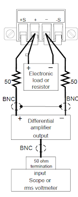
One thing that I wanted to do in the video but was not able to for brevity’s sake was talk about the differential amplifier.  The differential amplifier is important for two key reasons.  The first reason is that the differential amplifier will greatly reduce the common mode noise on the output.  This is important because you want to measure the noise between the outputs.  The other benefit of the differential amplifier is that it multiplies the output by 10.  This multiplication enables us to use more accurate ranges in both the scope and the RMS voltmeter which is very important when you want to keep the measurement uncertainties of your measurements down.


When you do the noise test, typically you do it at the full power point.  To get the full current, you can either use an electronic load or a fixed resistor.  Typically on a lower noise supply (such as the N6761A) you want to use a fixed resistor since the electronic load will introduce its own noise to the measurement.  This is not really an issue for power supplies with higher noise because their output noise is higher than the noise from the load.  In all honesty, it also tends to be difficult to find 500 W resistors so the load is a great help in those instances too!


The last measurement item that I want to talk about is the scope setup.  The scope should be AC coupled and have the filter turned on (since we only specify noise to 20 MHz, we want to filter anything above this out). We recommend that you put the scope in peak detect mode and turn the statistics so that you can see the highest and the lowest voltages recorded.    This will give you the true variation in the power supply output.  Your peak to peak voltage noise will be this difference divided by the gain of the diff amp.  After taking the peak to peak measurement, I typically move the connector over to the RMS voltmeter to take that measurement.  There are no special settings for the RMS voltmeter, you just need to remember to divide by the gain of the differential amplifier.

That is a really quick overview of voltage noise.  Please feel free to leave any questions in the comments section of this blog.   


Wednesday, November 21, 2012

How can I get more power from my power supplies?

If you need more voltage than one of your power supply outputs can provide, you can put power supply outputs in series to increase the total voltage. If you need more current than one of your power supply outputs can provide, you can put power supply outputs in parallel to increase the total current. However, you do have to take some precautions with series or parallel configurations.

Precautions for series connections for higher voltage:
  • Never exceed the floating voltage rating (output terminal isolation) of any of the outputs
  • Never subject any of the power supply outputs to a reverse voltage
  • Connect in series only outputs that have identical voltage and current ratings
Precautions for parallel connections for higher current:
  •  In most applications, one output must operate in constant voltage (CV) mode and the other(s) in constant current (CC) mode
  •  In most applications, the load on the output must draw enough current to keep the CC output(s) in CC mode
  • Connect in parallel only outputs that have identical voltage and current ratings

You can use remote sensing with either a series or parallel configuration. Figure 1 shows remote sensing for series outputs and Figure 2 shows remote sensing for parallel outputs.


You can find more information about power supply series and parallel configurations in an Agilent document called “Ten Fundamentals You Need to Know About Your DC Power Supply” by clicking on this link:
Refer to tip number 4 on page 6. This document also covers nine other useful power supply fundamentals.

Thursday, November 15, 2012

Validating battery capacity under end-use conditions for battery powered mobile devices


One aspect (of many) I have talked about for optimizing battery life for battery powered mobile devices is assessing the battery’s actual capacity. Not only do you need to assess its capacity under conditions as stated by the manufacturer but also under conditions reflecting actual end use.

Validating the battery under a manufacturer’s stated conditions establish a starting point of what you might be achievable in how much capacity you can obtain from the battery and if it is in line with what the manufacturer states. Sometime it can be less for a variety of reasons. Even subtle differences in stated conditions can lead to fairly substantial differences in capacity. The stated conditions usually provide a “best case” achievable value for capacity. Do not be surprised if your results for the battery’s capacity fall a little short of the best case value provided by the manufacturer. With a little work you may be able to determine what subtle difference caused it, or simply, the best case value given is a bit optimistic.

Validating the battery under end-use conditions helps establish the difference you can expect between the battery’s capacity for rather ideal stated conditions against end-use conditions. Battery powered mobile devices draw current in a pulsed fashion, with high peaks in relation to the overall average current drain. An example of this kind of dynamic current drain is shown in Figure 1. In this case it is the active mode current drain of a GPRS smart mobile phone.


Figure 1: GPRS smart mobile phone dynamic current drain waveform

This usually significantly degrades the battery’s delivered capacity in comparison to the manufacturer’s stated conditions, which are based on a constant DC current discharge. If you do not take the impact of end-use loading conditions on the battery’s capacity into account there is a good chance the mobile device’s run-time will fall quite a bit short of expectations.

The usual way to validate a battery’s capacity under end-use conditions is to actually hook the battery together with its device, connect up logging instrumentation for recording the battery run down voltage and current over time, and then placing the device in a desired operating mode and let it run until the battery is run down. While a battery run-down test like this is useful to do it has a couple of issues when trying to focus explicitly on just the battery:
  • It is a test of the combination of the battery together with its host device. The host device also has influence on the test’s outcome and must be taken into account in assessing just the battery under end-use.
  • It can often be complex and difficult to set up the device in its desired operating condition, requiring a substantial amount of supporting equipment to recreate its environment for providing a realistic operating condition.
  • It can sometimes be difficult to get consistently repeatable results with the actual device.

An alternative to repeatedly using the actual device is to use an electronic load that can draw a dynamic current representative of the actual device the electronic load is being used in place of. In some cases a simple low duty cycle, high crest factor pulsed current waveform can be directly programmed into the electronic load. In cases where the host device’s current drain waveform is a bit more complex it may be useful to have an electronic load that is able to “play back” a digitized waveform file that is a representative portion of the device’s actual current drain, on an ongoing basis to run down the battery. As one example we put features into our 14585A software to simplify this record and playback approach using our N6781A 2-quadrant DC source measure module. This set up is depicted in Figure 2.


Figure 2: Current drain record and playback set up using the 14585 and N6781A

In the first half of this process the N6781A serves as a voltage source to power up the device while digitizing its dynamic current drain waveform. In the second half of this process the captured current drain waveform is inverted and then played back by the N6781A now instead operating as a constant current load connected to a battery to discharge it. A colleague in our office recently completed a video of how to do this record and playback process using a digital camera as an example, capturing the current drain waveform of the process of taking a picture. This could be played back repeatedly to determine how many pictures could be taken with a set of batteries, for example. I know with my digital camera I need to take a spare set of batteries with me as it uses up batteries quite quickly! The video is available to be viewed at the following link:“record and playback video”

Thursday, November 8, 2012

Configuring an Electronic Load for Zero Volt Operation


DC electronic loads are indispensable for testing a variety of DC power sources. There are a number of situations that call for testing DC power sources at low voltage, even right down to zero volts. Often this is also at relatively high current of many tens of amps or greater. Some examples include:
  • Low output voltage power supplies and DC/DC converters (mostly for digital circuit power)
  • Solar cell I-V testing, down to zero volts
  • Fuel cell testing
  • Single cell battery testing
  • Power supply true output short-circuit testing, down to zero volts


It becomes challenging for the test engineer to find adequate DC electronic loads for low voltage operation, especially at high currents. Many DC electronic loads, including the ones Agilent Technologies provides, use multiple power FETs for their input loading element. While a power FET can actually operate down to zero volts, this is at zero current as well. At high current a few volts is typically needed for stable, dynamic operation at full current.  As one example Figure 1 depicts the input I-V characteristics of an Agilent N3304A DC electronic load.


Figure 1: Agilent N3304A DC electronic load input I-V characteristics

An effective solution for low voltage electronic load operation, right down to zero volts, for the electronic load’s full rated current, is to connect a low voltage boost power supply in series with the electronic load’s input. An example of this set up is depicted in Figure 2.


Figure 2: Zero volt DC electronic load set up

The electronic load now sees the sum of the boost supply’s and DUT’s voltages. Selecting a boost supply having adequate voltage will assure the electronic load will be able to operate at full performance at full current, even when the voltage at the DUT is zero. There are a few things that need to be paid attention to:
  • The electronic load needs to dissipate the total power of both the boost supply and DUT
  • The DUT needs to be adequately safeguarded against reverse polarity if the electronic load is inadvertently turned on too hard
  • The electronic load’s voltage sensing must be able to accommodate the extra voltage difference between the electronic load and DUT, due to the boost supply voltage
  • The boost supply ripple and noise (PARD) can contribute to noise measurements made on the DUT


Due to these considerations not all electronic loads may be well suited for zero volt operation with a boost supply so it is necessary to validate if a particular electronic load under consideration can be applied in this manner first.  Further details about zero voltage load operation as well as using Agilent N3300 series DC electronic loads for this purpose are described in product note “Agilent Zero Volt Electronic Load”, publication number 5968-6360E. Click here to access

Wednesday, October 31, 2012

What happens if remote sense leads open?

Remote sense is a feature on many power supplies that allows the power supply to regulate its output voltage right at your load (“remotely”) instead of at the power supply output terminals. Use remote sense when you want to compensate for load lead voltage drop caused by load current flowing in your load leads. This is accomplished by using a pair of remote sense leads that are in addition to your load leads. See an example in Figure 1. The power supply uses the voltage across the remote sense lead terminals to sense (measure) the voltage at the load terminals and regulate the voltage directly across the load by adjusting the output terminal voltage. Refer to this post I wrote last year on remote sense:
http://powersupplyblog.tm.agilent.com/2011/08/use-remote-sense-to-regulate-voltage-at.html


Remote sense leads could be accidentally left open, or once connected, one or both leads could inadvertently become open. I have had users of our power supplies testing very expensive devices under test (DUTs) ask me what would happen to the output voltage if a sense lead wired in a system opened; they were worried about subjecting their very expensive DUT to excessive voltage.

To understand why this is an important consideration, it is necessary to better understand the role of the sense leads. To regulate its output voltage, a power supply uses internal circuitry that acts as a feedback loop. The voltage is set to a particular value and the feedback loop monitors (measures) the voltage across the sense terminals and compares it to the setting. If it is too low, the loop circuitry increases the output voltage. If it is too high, the loop circuitry decreases the output voltage. So the actions of this loop result in the output voltage settling (being regulated) at a value such that the sense lead voltage equals the voltage set point.

If one or both of the sense leads is open, the feedback loop is broken and incorrect voltage information is sent to the loop. With an open sense lead, the sense voltage is typically near zero. The loop thinks the output voltage is too low and responds by increasing the output voltage. But this does not result in a corresponding increase in the sense lead voltage since the wire is broken so the loop increases the output voltage more. This continues until the value is increased to the maximum amount possible, which is usually somewhat higher than the maximum rated voltage of the power supply and very much beyond the desired set point. This could easily damage the DUT!

The scenario described in the previous paragraph is what would happen if no action was taken to prevent a runaway output voltage due to an open sense lead. Agilent power supplies have an internal circuit, called open sense protection, that prevents the output voltage from rising significantly above the set voltage if one or both of the remote sense leads is open. In fact, with one or both sense leads open, the output voltage of most Agilent power supplies will rise only 1 or 2 percent above the setting. Additionally, some Agilent power supplies can detect an open sense lead and respond by shutting down the output and alerting the user by changing a bit in a status register.

Note that this open sense protect circuitry is in addition to and independent from the over-voltage protection (OVP) circuitry common on most Agilent power supplies. OVP is a setting that is separate from the output voltage setting. If the actual output voltage exceeds the OVP setting, the OVP will shut down the output to protect the DUT.

Friday, October 26, 2012

What is a bipolar (four-quadrant) power supply?

To answer this question, I have to start with a basic definition of polarity conventions. Figure 1 shows a simple diagram of a power supply (a two-terminal device) with the standard polarity for voltage and current. A standard power supply typically is a source of power. To source power, current must flow out of the positive voltage terminal. Most power supplies source energy in this way by providing a positive output voltage and positive output current. This is known as a uni-polar power supply because it provides voltage with only one polarity. By convention, the “polarity” nomenclature typically refers to the polarity of the voltage (not the direction of current flow).
If current flows into the positive voltage terminal, the power supply is sinking current and is acting like an electronic load – it is absorbing and dissipating power instead of sourcing power. Most power supplies do not do this although many Agilent power supplies can sink some current to quickly pull down their output voltage when needed – this is known as a down-programmer capability – see this post for more info: http://powersupplyblog.tm.agilent.com/2012/03/if-you-need-fast-rise-and-fall-times.html.

To fully define power supply output voltage and current conventions, a Cartesian coordinate system is used. The Cartesian coordinate system simply shows two parameters on perpendicular axes. See Figure 2.  By convention, the four quadrants of the coordinate system are defined as shown. Roman numerals are typically used to refer to the quadrants. For power supplies, voltage is normally shown on the vertical axis and current on the horizontal axis. This coordinate system is used to define the valid operating points for a given power supply. A graph of the boundary surrounding these valid operating points on the coordinate system is known as the power supply’s output characteristic.
As mentioned earlier, some power supplies are uni-polar (produce only a single polarity output voltage), but can source and sink current. These power supplies can operate in quadrants 1 and 2 and can therefore be called two-quadrant supplies. In quadrant 1, the power supply would be sourcing power with current flowing out of the more positive voltage terminal. In quadrant 2, the power supply would be consuming power (sinking current) with current flowing into the more positive voltage terminal.

Some power supplies can provide positive or negative voltages across their output terminals without having to switch the external wiring to the terminals. These supplies can typically operate in all four quadrants and are therefore known as four-quadrant power supplies. Another name for these is bipolar since they are able to produce either positive or negative voltage on their output terminals. In quadrants 1 and 3, a bipolar supply is sourcing power: current flows out of the more positive voltage terminal. In quadrants 2 and 4, a bipolar supply is consuming power: current flows into the more positive voltage terminal. See Figure 3.
Agilent’s N6784A is an example of a bipolar power supply. It can source or sink current and the output voltage across its output terminals can be set positive or negative. It is a 20 W Source/Measure Unit (SMU) with multiple output ranges. See Figure 4 for the output characteristic of the N6784A.
To summarize, a bipolar or four-quadrant power supply is a supply that can provide positive or negative output voltage, and can source or sink current. It can operate in any of the four quadrants of the voltage-current coordinate system.

Monday, October 15, 2012

Flyback Inverter for Fluorescent Lamp: Part 2, A Little Theory of Operation


In part 1 of this posting “Flyback Inverter for Fluorescent Lamp: Part 1, Making Repairs” a little careful and straightforward troubleshooting and repair brought my friend’s fluorescent lamp assembly back to life again. But a fluorescent lamp has quite a few unique requirements to get it to start up and stay illuminated. How does this flyback converter manage to do these things?

I had first looked around to see if I could find a schematic for this fluorescent lamp assembly, but nothing turned up for me. However, the parts count was low enough, and circuit board large enough, that it was a fairly simple matter to trace out and sketch the inverter’s schematic in fairly short order, as shown in Figure 1.


Figure 1: Fluorescent lamp single-ended flyback inverter circuit


When first powered up the switching transistor is biased on by the 812 ohm resistor, energizing transformer winding W1. This in turn applies positive feedback to the transistor through winding W2, driving it into saturation. There are two mechanisms in the flyback transformer that are critical for making this inverter work:
  • First it has a gapped core. This allows it to store a substantial amount of energy in its magnetic field which in turn gets dumped over to the fluorescent tube through the secondary winding W3 when the transistor turns off and the transformer’s magnetic field collapses.  During this period the winding voltage continues to climb as the magnetic field collapses until the energy can find a place to discharge to, in this case into the fluorescent tube. The voltage is also further increased by the turns ratio of the transformer. This is the “flyback” effect that creates sufficiently high enough voltage to get the fluorescent tube to “strike” or ionize its gas to get it to start conducting and give off illumination, typically many hundreds of volts.
  • As can be seen this inverter is a very simple circuit with a minimum of parts. A second mechanism in the transformer is it is designed to saturate in order to make the inverter oscillate. At the end of the transistor’s “on” period the transformer reaches its maximum magnetic flux at which point the transformer saturates. Winding voltage W2 drops to zero and then reverses driving the switching transistor into cutoff.  After the magnetic field has collapsed and energy discharged to the fluorescent tube the process repeats itself.


The switching transistor’s collector and base voltages during turn on are captured in the oscilloscope diagram shown in Figure 2.


Figure 2: Inverter switching transistor collector and base voltage waveforms

A number of interesting things can be observed in Figure 2.  The oscillation period is roughly 50 microseconds, or oscillation frequency of 20 kHz. It takes about 10 cycles, 500 microseconds, for the fluorescent tube to strike. During this initial phase the peak collector voltage is flying up to nearly 100 volts or about 8 times the DC input voltage being applied. Again, this voltage is being multiplied up by the turns ratio of windings W1 and W2 to bring this up in the vicinity of 600 volts or so needed to make the fluorescent tube to strike. Once the tube does strike and starts conducting its impedance drops. This causes the collector voltage to drop down to about 35 volts which is consistent with the proportion of drop in voltage needed for the fluorescent tube once it’s gas is ionized and is conducting. Note also the collector voltage pulse also widens as it takes a longer time for the energy in the transformer to be dumped when it’s at a lower voltage.

Although this inverter at first glance is a rather simple and minimum viable, minimum parts count circuit, with careful design it can be made to be very efficient. This is where the design of the transformer becomes as much art as science, knowing how the subtle characteristics of the magnetic material and inductive and capacitive parasitics can be used to advantage in contributing to and improving the overall performance of the design.

Anyway, what my friend really cared about is the lamp now works and he is able to put it to good use in his camper!