Showing posts with label Usage. Show all posts

Friday, October 31, 2014

APS Paralleling Made Easier through Programming

Hi Everyone,

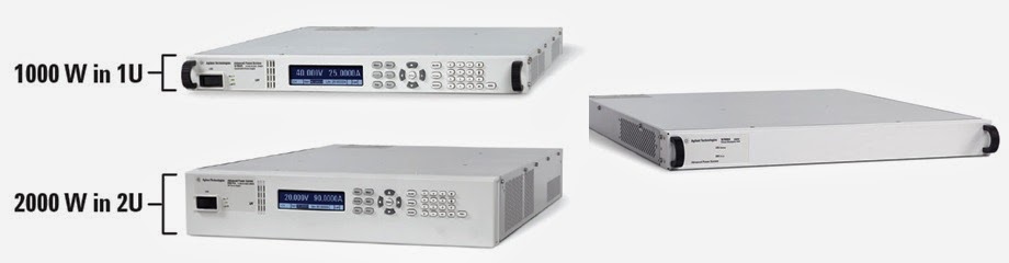
The Advanced Power Supply family has a very slick way to parallel units for higher current called current sharing.  This enables all of the paralleled units to be in Constant Voltage (CV) mode which is a change from most of our other power supplies that have one unit in CV mode and the rest of the units in Constant Current (CC) mode.  My colleague Ed did a very informative blog post about the different paralleling options that explains a bit more about paralleling units so I will not rehash any of that here.  Here is a link to that post: Paralleling Power Supplies.

The main drawback of the paralleling on the APS is that it can be a little difficult to get everything properly set to get the best performance.  You need to synchronize your current measurements and your voltage transients.  If you look in the manual, there are quite a few pages explaining how to set this all up.  I am happy to say that we have made this a little easier.  Our summer intern spent some time writing a VBA program in Excel that automatically does much of this.  The program uses Keysight VISA-COM so you need to have the Keysight IO Libraries installed to use it.  It will work with LAN, GPIB, and USB (all of which come standard on all APS units).

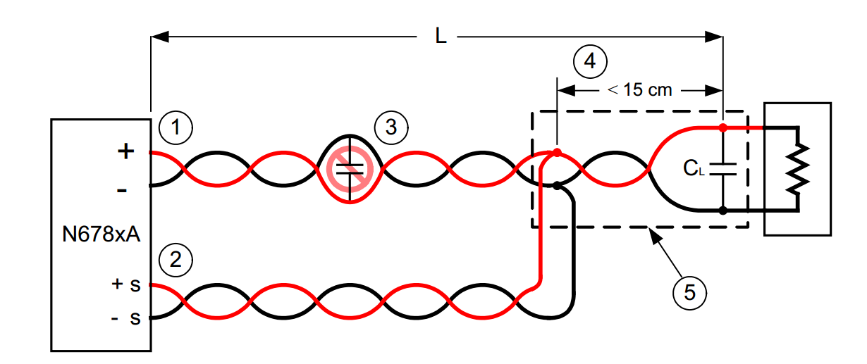
The first thing that we need to do is talk about the setup.  There are quite a few wire connections that need to be made.

First you need to connect the current sharing ports, the sense connections, and the outputs to the load:

After that, you also need to make some connections on the 8 pin  digital connector on the back of the APS units. You do not need to worry about setting up the pins if you plan on using the default pin assignments from the program.  The default pin assignments are:

Pin 6 on all units - On Couple
Pin 7 on all units - Off Couple
Pin 1 on the master unit - Trigger Out
Pin 1 on all other units - Trigger In
Pin 8 on all units - common

Here is a wiring diagram of the default assignments (for 3 units):


The On/Off Couple Pins make it so that when you enable or disable the output on any unit, all of the units enable or disable. The trigger line enable us to synchronize measurements as well as voltage changes.  

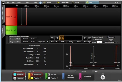
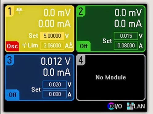
The Interface looks something like this:

It is divided into four boxes.  I will refer to them as boxes 1 to 4 with 1 being the left most box.  Box 1 is where you enter the VISA initialization string for each paralleled supply.  You can get this from the Keysight IO Libraries.  Box 2 is where you enter your settings  You can set the voltage limit, positive and negative current limit, change the output state, and change the voltage.  Most importantly, this is where you set the number of paralleled units.  This needs to be done or else the program will not work correctly.  You can parallel 1 kW and 2 kW units with each other, as long as they have the same maximum voltage so we also need to break out the number of 2 kW units in the scheme.  The third box will do a scalar measurement of the voltage and current.  This will report the total current of the paralleled units (it does a triggered measurement and adds all of the current measurements).  The fourth box will measure arrays of current and voltage (this function will not work on the N6900 APS units).      

I have posted this program on our Keysight Power Supply Forums at: Matt's Forum Post.  I have also opened a thread there where we can discuss this program.  It is still kind of preliminary so any feedback could possibly be incorporated into the program.  

That is all I have for this month.  Happy Halloween to all of our readers and please let me know any comments in the forum.


Wednesday, October 15, 2014

Creating a "bumping" auto-restarting over current protect on the N6900A/N7900A Advanced Power System

The two main features in system power supplies that have traditionally protected DUTs from too much current are the current limit and the over current protect (OCP). When a device, for any of a number of reasons, attempts to draw too much current, the current limit takes control of the power supply’s output, limiting the level of current to a safe level. An example of current limit taking control of a power supply output is shown in Figure 1.


Figure 1: Current limit protecting a DUT against excess current.

For those devices that cannot tolerate a sustained current at the current limit level, the over current protect can be set and activated to work with the current limit and shut down the power supply output after a specified delay time. This will protect a DUT against sustained current at the limit.  An example of an OCP shutting down a power supply output for greater protection against excess current is shown in Figure 2.


Figure 2: OCP protecting a DUT against excess current

We have talked about the current limit and OCP in previous posts. For more details on how the OCP works, it is worth reviewing “What is a power supply’s over current protect (OCP) and how does it work?” (Click here to review)

Sometimes it is desirable to have something that is in between the two extremes of current limit and OCP.  One middle-ground is a fold-back current limit, which cuts back on the current as the overload increases. More details about a fold-back current limit are described in a previous posting “Types of current limits for over-current protection on DC power supplies” (Click here to review). One thing about a fold-back current limit is the DUT and power supply will not be able to recover back into constant voltage (CV) operation unless the DUT is able to cut way back on its current demand.

Another type of current limit behavior that operates between regular current limit and OCP is one that shuts down the output, like OCP, but only temporarily. After a set period of time it will power up the output of the power supply again. If the DUT is still in overload, the power supply will shut down again. However, if the DUT’s overload condition has gone away, it will be able to restart under full power. In this way the DUT is protected against continuous current and at the same time it the power supply is not shut down and requiring intervention from an operator.

While this type of current limit is not normally a feature of a system DC power supply, it is possible to implement this functionality in the N6900A/N7900A Advanced Power System (APS) using its expression signal routing feature. This is a programmable logic system that is used to configure custom controls and triggers that run within the APS. Here the expression signal routing was used to create an auto-restarting current shutdown protect in the example shown in Figure 3.


Figure 3: Custom auto-restarting current shutdown protect configured for N6900A/N7900A APS

A custom control was created in the expression signal routing that triggers the output transient system to run if the current limit is exceeded for longer than 0.3 seconds. A list transient was programmed into the APS unit to have its output go to zero volts for 10 seconds and then return to the original voltage setting each time it is triggered. In this way the output would pulse back on for 0.3 seconds and then shut back down for another 10 seconds if the overload was not cleared. The custom trigger signal was graphically created and downloaded into the APS unit using the N7906A software utility, as shown in Figure 4.


Figure 4: Creating custom trigger for auto-restarting current shutdown protect on APS

Current limit and over current protect (OCP) are fairly standard in most all system DC power supplies for protecting your DUT against excess current. There are not a lot of other choices beyond this without resorting to custom hardware. One more option now available is to make use of programmable signal routing like that in the N6900A/N7900A APS. With a little ingenuity specialized controls like a auto-restarting current shutdown protect can be created through some simple programming.

Monday, October 6, 2014

Simulating battery contact bounce, part 2

In part 1 of this posting on simulating battery contact bounce (click here to review) I discussed what battery contact bounce is about and why creating a voltage dropout may not be adequate for simulating battery contact bounce. The first answer to addressing this was provided; use a blocking diode and then a voltage dropout is certain to be suitable for simulating battery contact bounce.

Another approach for simulating battery contact bounce is to add a solid state switch between the DC source and the battery powered device. While this is a good approach it is complex to implement. A suitable solid state switch needs to be selected along with coming up with an appropriate way to power and drive the input of the switch need to be developed.

If for some reason using a blocking diode is not suitable, there is yet another fairly simple approach that can be taken to simulate high impedance battery contact bounce. Instead of programming a voltage dropout on the DC source, program a current dropout. Where the voltage going to zero during a voltage dropout is effectively a short circuit, as we saw in part 1, the current going to zero during a current dropout is effectively an open circuit. There are a couple of caveats for doing this. The main one is battery powered devices are powered from a battery, which is a voltage source, not a current source. In order for the DC source to act as a voltage source when delivering power, we need to rely on the DC source voltage limit being set to the level of the battery voltage. In order for this to happen we need to set the non-dropout current level to be in excess of the maximum level demanded by the device being powered and. Thus the DC source will normally be operating in voltage limit. Then when the current dropout drives the output current to zero, the DC source switches its operating mode from voltage limit to constant current, with a current value of zero. This operation is depicted in Figure 4, using a Keysight N6781A 2-quadrant SMU module designed for testing battery powered devices, operating within an N6705B DC Power Analyzer. In this example the current ARB for the dropout was both programmed and the results shown in Figure 1 captured using the companion 14585A software.


Figure 1: Current ARB creates a high impedance dropout to simulate battery contact bounce

Another caveat with using this approach for simulating battery contact bounce is paying careful attention to the behavior of the mode crossovers. For the first crossover, from voltage limit to constant current operation (at zero current) there is a small amount of lag time, typically just a fraction of a millisecond, before the transition happens. This becomes more significant only when trying to simulate extremely short contact bounce periods. More important is when crossing back over from constant zero current back to voltage limit operation. There is a short period when the current goes up to its high level before the voltage limit gains control, holding the voltage at the battery’s voltage level. Usually any capacitance at the input of the DUT will normally absorb any short spike of current. If this crossover is slow enough, and there is very little or no capacitance, the device could see a voltage spike. The N6781A has very fast responding circuits however, minimizing crossover time and inducing just 250 mV of overshoot, as is seen in Figure 1.

Hopefully, now armed with all of these details, you will be able to select an approach that works best for you for simulating battery contact bounce!


Tuesday, September 30, 2014

How Do I Properly Wire My Output?

Hi everyone,


September has been a hectic month here at Keysight’s Power Supply Headquarters (to give you an idea of the kind of month it has been, my dog literally ate my passport a week before I left on an international trip) but I am back with another blog post for your reading pleasure.  Today we are going to talk about how to properly wire your power supply.  This is a common question.  Wiring is something that on the surface seems like it should be really easy but when you dig a little deeper there are many layers to consider.  The repercussions can be pretty severe as well.  With improper wiring, you can make a high performance power supply seem like a low performance benchtop supply.

First, let's talk about the things repercussions of improper wiring.  The first and probably most undesired result is that your voltage will be unstable.  I have seen this in my own former career as a test engineer.  The inductance from our wiring coupled with some capacitance in our test equipment resulted in an oscillation that caused a test to fail.  We spent a Saturday chasing this down and fixed it by properly wiring our system.   

The second undesired result is that your voltage rise time and fall times could be much longer than specified.  This will negatively affect your test throughput which in high volume manufacturing test could cost money due to increased test time.   Properly wiring your power supply will enable you to get the maximum throughput from your power supply.  

The last repercussion that I'll discuss is voltage overshoots and undershoots.  You want these to be as small as possible.  A large overshoot can possibly damage your DUT especially if you do not have your over voltage properly set. A voltage undershoot could cause your DUT to shut down due to a low voltage condition. 

All of these are real pains when you are trying to get your test set up and running.  There are ways to properly wire your system so you can get the maximum specs out of your power supply.  

The first and most basic wiring tip is to keep the wiring as short as possible.  The longer the wiring the higher the impedance from the wiring will be.  The table below shows some specifications on some standard wire sizes:


The second tip is to use remote sensing.  This will sense around all of the wiring drops from the wiring.  This is good practice at all times.  Remote sensing is cool.

The third tip is to twist your wires together.  The key thing to remember her is that you twist the + and - output together and the + sense and - sense together.  This will reduce the mutual inductance in the wires.  Never, ever twist the sense and output leads together.  

This is a picture of the spool of wire that we use for our sense wires here.  You can see the the wires are very tightly twisted together here:

The other option is to use special low inductance wiring.  If you look at the below picture, you can see that there are two flat conductors separated by an insulator.  This reduces the mutual inductance even more than twisting the wires.:


Our N678xA SMU DC Power Modules are very sensitive to how they are wired.  Here is a diagram showing the proper wiring for the N678xA:


The top three items I mentioned should be standard practice when you set up your system.  These are just great wiring practices.  Sometimes you need to go the extra mile.  Back when I was in the test group we followed all of these tips as best I could but due to the test system, we could not minimize the wire length enough.  Our solution was to parallel more wires between the power supply and the load that we were using.  Instead of one twisted pair, we used three twisted pairs in parallel.  This also reduces the impedance of the wiring because you are paralleling the conductors (paralleled inductance and resistance reduces).

One of our design engineers wrote a very good article that touched on this subject a bit.  You can check that out here: Article Link.  

I hope that this is useful to everyone.  Please let us know if you have any questions or comments.


Monday, September 29, 2014

Properly sequence multiple power inputs to protect your DUT

As I mentioned in a previous post, we have devoted a lot of time writing about protecting your device under test (DUT) from the two main DUT-destroying forces available from a power supply: excessive voltage and excessive current. Click here for one of the latest posts including a list to the other posts.

Today I’d like to cover another topic that can cause DUT failure due to a power supply. Some DUTs have multiple DC inputs and some of these multiple-input DUTs are sensitive to the order in which the inputs turn on or turn off. Subjecting the device to an uncontrolled sequence could cause latch-up or excessive current to flow resulting in compromised reliability or even immediate catastrophic failure of the DUT. So properly sequencing the multiple voltages at turn on and off is essential. My colleague, Ed Brorein, wrote a very similar post last year (click here) but I thought this topic was worth repeating especially since we added another series of power products with higher power that has this capability.

Various methods have been used in an effort to address the potential problem associated with improperly sequenced power inputs. Diodes can be placed from one input to another to clamp the voltage thereby preventing one input voltage from going too far above or below another input voltage but this method has limited effectiveness and variable results. Relays can be put in series with each input and controlled with timing circuitry but the relays introduce variable series impedance and timing is imprecise. FETs with associated control circuitry can be placed in series with each input however this method requires significant design time and adds complexity to the setup. Multiple DC power supplies can be controlled through software, but once again, timing is imprecise and response times can be slow.

Several years ago, I wrote an application note on a closely related topic (click here). The method that is most precise and introduces the fewest complications is to use a power supply system that has output sequencing integrated into the system itself. Keysight has several power supply systems that can accommodate precise output sequencing: the N6700 Modular Power System, N6705 DC Power Analyzer, and the more recently released N6900/N7900 Advance Power System. Each system offers the ability to precisely control the turn-on and turn-off sequence of multiple outputs. Timing is set with sub-millisecond resolution. Synchronization across systems is also possible to facilitate timed shut downs of larger numbers of power supply outputs for your DUT inputs. The above mentioned application note specifically addressed the topic of how to configure the system to properly shut down your DC inputs in sequence upon a fault generated by any of the system power supplies.

Below is a simple example of a sequenced turn on of four outputs in an N6705B mainframe. The sequencing is facilitated by setting a different turn-on delay time for each of the outputs (turn-off delays can be set independently). When all outputs are told to turn on simultaneously, the delays are activated resulting in a precisely controlled sequenced turn on. Figure 1 shows how easy it is to implement the delays for a turn-on event. In this case, I used four power supply outputs in an N6705B mainframe with delays set to 5 ms, 10 ms, 15 ms, and 20 ms. I set the output voltages to 10 V, 7.5 V, 5 V, and 3.3 V. You can also set the output voltage rise time (slew rate) independently for each output. Figure 2 shows the results using the scope that is built into the N6705B mainframe.


So you can see that with the proper power supply system, sequencing your multiple DC power supply inputs on your device to protect it from damage is easy. Keysight provides you with the solution to do just that adding to our arsenal of features that protect your valuable DUT.

Wednesday, September 17, 2014

Simulating battery contact bounce, part 1

One test commonly done during design validation of handheld battery powered devices is to evaluate their ability to withstand a short loss of battery power due to being bumped and the contacts momentarily bouncing open, and either remain operating or have sufficient time to handle a shutdown gracefully. The duration of a contact bounce can typically range anywhere from under a millisecond to up to 100 milliseconds long.

To simulate battery contact bouncing one may consider programming a voltage drop out on a reasonably fast power supply with arbitrary waveform capabilities, like several of the N675xA, N676xA, or N678xA series modules used in the N6700 series Modular DC Power System or N6705B DC Power Analyzer mainframe, shown in Figure 1. It is a simple matter to program a voltage dropout of specified duration. As an example a voltage dropout was programmed in Figure 2 on an N6781A SMU module using the companion 14585A software.


 Figure 1: N6700 series and N6705B mainframes and modules


Figure 2: Programming a voltage drop out using the N6705B and N6781A SMU module

While a voltage dropout is fine for many applications, like automotive, in many situations it does not work well for simulating battery contact bounce. The reason for this is there is one key difference to note about a voltage dropout versus a battery contact bounce. During a voltage dropout the source impedance remains low. During a battery contact bounce the source impedance is an open circuit. However, a DC source having the ability to generate a fast voltage dropout is a result of it being able to pull its output voltage down quickly. This is due to its ability to sink current as well as source current. The problem with this is, for many battery powered devices, this effectively short-circuits the battery input terminals, more than likely causing the device to instantly shut down by discharging any carry-over storage and/or disrupting the battery power management system. As one example consider a mobile device having 50 microfarads of input capacitance and draws 4 milliamps of standby current. This capacitance would provide more than adequate carryover for a 20 millisecond battery contact bounce. However, if a voltage dropout is used to simulate battery contact bounce, it immediately discharges the mobile device’s input capacitance and pulls the battery input voltage down to zero, as shown by the red voltage trace in Figure 3. The yellow trace is the corresponding current drain. Note the large peaks of current drawn that discharge and recharge the DUT’s input capacitor.


 Figure 3: Voltage dropout applied to DUT immediately pulls voltage down to zero

One effective solution for preventing the DC source from shorting out the battery input is to add a DC blocking diode in series with the battery input, so that current cannot flow back out, creating high impedance during the dropout. This is illustrated in Figure 4.


Figure 4: Blocking diode added between SMU and DUT

One thing to note here is the diode’s forward voltage drop needs to be compensated for. Usually the best way to do this just program the DC source with the additional voltage needed to offset the diode’s voltage drop. The result of this is shown in Figure 5. As shown by the red trace the voltage holds up relatively well during the contact bounce period. Because the N6781A SMU has an auxiliary voltage measurement input it is able to directly measure the voltage at the DUT, on the other side of the blocking diode, instead of the output voltage of the N6781A. As seen by the yellow current trace there is no longer a large peak of current discharging the capacitor due to the action of the blocking diode.


 Figure 5: Blocking diode prevents voltage dropout from discharging DUT 

Now you should have a much better appreciation of the differences between creating a voltage dropout and simulating battery contact bounce! And as can be seen a blocking diode is a rather effective means of simulating battery contact bounce using a voltage dropout. Stay tuned for my second part on additional ways of simulating battery contact bounce on an upcoming posting.
.


Wednesday, September 10, 2014

How do I protect my DUT against my power supply sense lines becoming disconnected, misconnected, or shorted?

The remote sense lines are a vital part of any good system power supply. As shown in Figure 1, by using a second, separate pair of leads for sensing, the output voltage is now regulated right at the DUT rather than at the output terminals on the power supply. Any voltage drops in the force leads are compensated for; assuring the highest possible voltage accuracy is achieved right at the DUT.


Figure 1: Remotely sensing and regulating output voltage at the DUT

Of course for this to work correctly the sense leads need to have a good connection at the DUT. However, what if the sense leads become disconnected, misconnected, or shorted?

One might think if one or both of the sense leads became disconnected, the sensed voltage would then become zero, causing the output voltage on the force leads to climb up out of control until the over voltage protect (OVP) trips. This turns out not to be the case, as a co-contributor here, Gary had pointed out in a previous posting “What happens if remote sense leads open?” (Click here to review). Basically a passive protection mechanism called sense protect maintains a backup connection between the sense line and corresponding output terminal inside the power supply in the event of a sense line becoming disconnected.

While sense protect is an indispensable feature to help protect your DUT by preventing runaway over-voltage, if a sense lead is open the voltage at your DUT is still not as accurate as it should be due to uncompensated voltage drops in the force leads. This can lead to miscalibrated DUTs and you would not even know that it is happening. To address this some system power supplies include an active open sense lead fault detection system. As one example our 663xx Mobile Communications DC Sources check the sense lead connections during each output enable and will issue a fault protect and shut down the output if one or both sense leads become disconnected. It will also let you know which of the sense leads are disconnected. It can be enabled and disabled as needed. I had written about this in a previous posting “Open sense lead detection, additional protection for remote voltage sensing” (Click here to review).

Taking sense protection further, we have incorporated a system we refer to as sense fault detect (SFD) in our N6900A and N7900A Advanced Power System (APS). It can be enabled or disabled. When enabled it continually monitors the sense lead connections at all times. If it detects a sense fault it sets a corresponding bit in the questionable status group register as well as turn on status annunciator on the front panel to alert the user, but does not disable the output. Through the expression signal routing system a “smart trigger” can be configured as shown in Figure 2 to provide a protect shutdown on the event of a sense fault detection.  In all, sense fault detect on APS provides a higher level of protection and flexibility.


Figure 2: Configuring a custom opens sense fault protect on the N6900/N7900 APS

What happens if the sense leads become shorted? Unlike open sense leads, in this case the output voltage can rise uncontrolled. The safeguard for this relies on the over voltage protect system. The same thing happens if the sense leads are reversed. The power supply will think the output voltage is too low and keep increasing the output voltage in an attempt to correct it. Again the safeguard for this relies on the over voltage protect system. The N6900/N7900 APS does actually distinguish the difference when the sense leads are reversed by generating a negative OVP (OV-) fault, giving the user more insight on what the fault is to better help in rectifying the problem.

Remote voltage sensing provides a great benefit by being able to accurately control the voltage right at the DUT. Along with the appropriate safeguards against sense lead misconnections you get all the benefit without any of the corresponding risks!

Remote sense protect and sense fault detect were just two of many topics about in my seminar “Protect your device against power related damage during test” I gave last month. As it was recorded it is available on demand if you have interest in learning more about this topic. You can access the sign up from the following link: (Click here for description and to register)

Sunday, August 31, 2014

How do I transfer files from my DC Power Analyzer to my PC?

Hi everybody!

I got back from my vacation just in time to get my August blog post out.  We typically try to shy away from product specific blog postings here at Watt's Up but this is a topic that I get a bunch of questions on in my support job and this is a great place for me to address it.

The Keysight N6705B DC Power Analyzer has an internal flash drive that stores information such as datalogs and scope waveforms.  When we first came out with the N6705B, it had a 64 MB drive (it is crazy how small that seems today).  Present N6705Bs have a 4 GB drive in them.  Since you can create datalogs of up to 2 GB in size, even a 4 GB drive can get full.  Today I am going to talk about how to get a file out of the internal drive of the N6705B and onto your PCs hard drive.

The way that I see it, there are three ways to get a file off the N6705B:

  1. The old fashioned way: You use a thumb drive and manually transfer the files that way.  The disadvantage here is that you need to have a thumb drive and there is no way to automate the process.
  2. You can use the N6705B LXI web interface.  There's a utility there that can transfer files bwtween the N6705B and your PC.  The disadvantages of this are that you cannot automate it and you can only do this if you are connected via LAN.
  3. There is a command (MMEM:DATA?) that will read back the contents of a file so you could write a SCPI program to do this.  This disadvantage here is that you need to write a program.  Luckily, I have done this in the past myself and I am more than willing to help!
Quite a few years ago, I wrote a VB 6 program that does number three.  The binary data for the file is in IEEE binary block format.  I find that the easiest way to read and write data in this format is to use Keysight VISA-COM and use the ReadIEEEblock function.  Here is a screen shot of my program listing:


As you can see in the program, I basically read the contents of the file default.dlog into filedata which I have dimensioned as  a byte array.  After I read all the data in, I kill any null data in the array and then copy it into a file that I have stored on my hard drive.  All in all, if you use this method it is pretty easy.

That's all I have for this month.  Please let me know if you have any questions or if you have discovered another way to transfer files.


Wednesday, August 20, 2014

Some differences between constant current (CC) and constant resistance (CR) loading on your DUT’s performance

Most electronic loads provide constant current (CC), constant resistance (CR) and constant voltage (CV) loading. Some also offer constant power (CP) loading as well. The primary reason for this is this gives the test engineer a choice of loading that best addresses the loading requirement for the DUT, which invariably is some kind of power source.

Most usually the device should be tested with a load that reflects what the loading is like for its end use. In the most common case of a device being predominantly a voltage source the most common loading choices are either CC or CR loading, which we will look at in more detail here. Some feel they can be used interchangeably when testing a voltage source. To some extent this is true but in some cases only one or the other should be used as they can impact the DUT’s performance quite differently.

Let’s first consider static performance. In Figure 1 we have the output characteristics of an ideal voltage source with zero output resistance (a regulated power supply, for example) and a non-ideal voltage source having series output resistance (a battery, for example).  Both have the same open circuit (no load) voltage. Superimposed on these two source output characteristics are two load lines; one for CC and one for CR. As can be seen they are set to draw the same amount of current for the ideal voltage source. However, for the non-ideal voltage source, while the CC load still continues to draw the same amount of current in spite of the voltage drop, not surprisingly the CR load draws less current due to its voltage-dependent nature.


Figure 1: CC and CR loading of ideal and non-ideal voltage sources

CC loading is frequently used for static power supply tests for a key reason. Power supplies are usually specified to have certain output voltage accuracy for a fixed level of current. Using CC loading assures the loading condition is met, regardless of power supply’s output voltage being low or high, or in or out of spec. Non-ideal voltage sources, like batteries, present a little more of a problem and are often specified for both CC and CR loading as a result, to reflect the nature of the loading they may be subjected to in their end use. Due to a battery's load-dependent output voltage, trying to use one type of loading in place the other becomes an iterative process of checking and adjusting loading until the acceptable operating point is established.

Let’s now consider dynamic performance.  CC loading generally has a greater impact on a power supply’s ability to turn on as well as its transient performance and stability, in comparison to CR loading. When the power supply first starts up its output voltage is at zero. A CR load would demand zero current at start up. In comparison a CC load still demands full current. Some power supplies will not start up properly under CC loading. With regard to transient response and stability, CR loading provides a damping action, increasing current demand when the transient voltage increases and decreases demand when the transient voltage decreases, because the current demand is voltage dependent. CC loading does not do this, which can negatively influence transient response and stability somewhat. Whether CC or CR loading is used depends on what the power supply’s specifications call out for the test conditions. Batteries have some dynamic considerations as well. Their output response can be modeled as a series of time constants spanning a wide range of time. This presents somewhat of a moving target for an algorithm that uses an iterative approach to settling on an acceptable operating point.


This is just a couple of examples of how a load’s characteristic affects the performance of the device it is loading, and why electronic loads have multiple operating modes to select from, and worth giving thought next time towards how your device is affected by its loading!

Tuesday, August 5, 2014

Upcoming Seminar on Protecting Your Device against Power-Related Damage during Test

Here on “Watt’s Up?” we have provided a good number of posts about various protection features incorporated into system power supplies to protect your device against power-related damage during test. Just recently my colleague Gary posted “How Does Power Supply Over-Voltage Work?” (Click here to review) Here he reviews inner workings of different OVP implementations.  I recently posted “Safeguarding Your Power-Sensitive DUTs against an Over-Power Condition” (Click here to review) Here I go over a method to protect your DUT against excess power when other power supply features like over current protection may be less than ideal.

The reason why we frequently share power-related protection topics here is protecting your DUT is extremely important, there are a lot of different capabilities incorporated in system power supplies for this purpose, and there are a lot of practical considerations when putting them to use.  

Hopefully a number of you have found our posts on protection-related topics of help. Because this is a very important topic and there is so much more you should know about it I will be giving a live web-based seminar “Protecting Your Device against Power-Related Damage during Test” on August 20th, just a few weeks away from today. I will be going over a number of protection-related topics which we have not yet covered here on “Watt’s Up?”.  One of my objectives is to provide a more holistic view of the many ways a system power supply is able to better safeguard against power-related damage as well as what is practical to expect when using these various capabilities incorporated in the power supply.

You can register online at the following (Click here for description and registration page) In case you are not able to attend the live event on August 20 you will be able to register and listen to seminar afterward as well, as it will be recorded.


So if protecting your device against power-related damage is important to you I hope you are able to attend the seminar!

Tuesday, July 22, 2014

What does it mean when my Agilent power supply displays “Osc”?

When using certain higher performance power supplies from Agilent, like the N678xA series source-measure modules, you may discover that the output has shut down and an annunciator displaying “Osc” shows up on the front panel meter display, like that shown in Figure 1 for the N6705B DC Power Analyzer mainframe. 


Figure 1: DC Power Analyzer front panel meter displaying “Osc” on channel 1 output

As you would likely guess, Osc stands for oscillation and this means the output has been shut down for an oscillation fault detection. In this particular instance an N6781A high performance source measure module was installed in channel 1 of the N6705B DC Power Analyzer mainframe.

The N678xA series source measure modules have very high bandwidth so that they can provide faster transient response and output slew rates. However, when the bandwidth of the power supply is increased, its output stability becomes more dependent on the output wiring and DUT impedances. To provide this greater bandwidth and at the same time accommodate a wider range of DUTs on the N678xA modules, there are multiple compensation ranges to select from, based on the DUT’s input capacitance, as shown in the advanced source settings screen in Figure 2.


Figure 2: DC Power Analyzer front panel displaying advanced source settings for the N678xA

Note that “Low” compensation range supports the full range of DUT loading capacitance but this is the default range. While it provides the most robust stability, it does not have the faster response and better performance of the “High” compensation ranges.

As long as the wiring to the DUT is correctly configured and an appropriate compensation range is selected the output should be stable and not trip the oscillation protection system. In the event of conditions leading to an unstable condition, any detection of output oscillations starting up quickly shut down the output in the manner I captured in Figure 3. I did this by creating an instability by removing the load capacitance.


Figure 3: Oscillation protection being tripped as captured in companion 14585A software

In rare circumstances, such as with some DUTs drawing extremely high amplitude, high frequency load currents, which may lead to false tripping, the oscillation protection can be turned off, as shown in Figure 4.


Figure 4: N678xA oscillation protection disable in N6705B DC Power Analyzer advance protection screen

Oscillation protection is a useful mechanism that can protect your DUT and your power supply from an excessively high AC voltage and current due to unstable operating conditions. Now you know what it means next time you see “Osc” displayed on the front panel of you Agilent power supply and what you need to do to rectify it!

.

Monday, July 14, 2014

Extending the usable bandwidth of the DC source when performing AC disturbance testing on your DUT

A lot of various products that run off of DC power, often destined to be used in automobiles and other types of vehicles, but even quite a number in stationary applications as well, require validation testing for impact of having AC disturbances riding on top the DC powering them.

 Conducting this type of testing is often a big challenge for the test engineer in finding a solution that adequately addresses the disturbance test requirements. It usually requires multiple pieces of hardware:
  • A DC power supply is used to provide the DC bias voltage and power.
  • A power amplifier is used to generate the AC disturbance.
  • A separate ARB /function generator is needed to produce the reference signal for the disturbance

Coupling the DC power supply and power amplifier together is extremely problematic. While it would be great to just directly connect the two in series, this rarely can be done in practice as the power amplifier usually cannot handle the DC current of the power supply. A variety of custom approaches are then typically taken, all with their associated drawbacks.

An article about this very topic was published last year, written by a colleague I work with, Paul Young in our R&D group. As he noted it’s great when the power source can provide both the DC power as well as the AC disturbance as this is a big savings over trying to incorporate multiple pieces of equipment. Paul’s article “Extending the Usable Bandwidth of a Programmable Power Supply for Generating Sinusoidal Waveforms” (click here to review) is an excellent reference on this and the inspiration for my blog posting this week.

Our N6705B DC Power Analyzer in Figure 1 and recently introduced N7900A series Advanced Power System (APS) 1KW and 2KW power supplies in Figure 2 have proven to be very useful for doing a variety of testing where transients and audio disturbances are needing to be introduced on top of the DC that is powering the DUT.


Figure 1: Agilent N6705B DC Power Analyzer and N6700 series DC power modules


Figure 2: Agilent N7900A series 1KW and 2KW Advanced Power System and N7909A Power Dissipator

The reasons for these products being useful for disturbance testing are due to their built in ARB generation capability in conjunction with having a respectable AC bandwidth, on top of being able to source the DC power. Everything can be done within one piece of equipment.

A very common test need is to superimpose a sinusoidal disturbance in the audio range. One example of this is in automobiles. The alternator “whine” AC ripple induced on top of the DC output falls within this category. Our 1KW and 2KW N7900A series APS are good for applications needing higher DC power. However, at first glance the specified AC bandwidth of 2 kHz on does not look like it would work well for higher audio frequencies. The AC response of an N7951A from 1 kHz to 10 kHz is shown in Figure 3. This was captured using the 14585A companion software to set up its ARB.  There is noticeable roll off for higher frequency, as expected.


Figure 3: N7951A APS AC response characteristics captured using companion 14585A software

However, it’s worth noting that the roll off is gradual and very predictable. In the case of superimposing a relatively small AC signal on top of the DC output it is easy to compensate by measuring the attenuation at the given frequency and applying a gain factor to correct for it, as I did as shown in Figure 4. As one example, for 5 kHz, I programmed 2.38 volts peak to get the desired 1 volt peak.


Figure 4: N7951A APS AC response characteristics after gain correction

As can be seen it was simple to now get a flat response over the entire range. A limiting factor here is sum of the programmed DC value plus programmed AC peak value needs to be within the voltage programming range of the power supply being used. In practice, when the AC disturbance is reasonably small it is easy to cover a wide range of frequency.

Another factor to consider is capacitive loading. Some DC powered products sometimes have a fairly substantial filter capacitor built in across the DC power input. This will increase the peak current drain from the power supply when AC is applied on top of the DC. As an example a 100 microfarad capacitor will draw a peak current of 6.28 amps when a 10 kHz, 1 volt peak AC signal is applied. There may also be series impedance limiting the peak current, but whatever this AC peak current is it needs to be included when determining the size of the power supply needed.

With these basic considerations you will be able to perform AC disturbance testing over a much greater bandwidth as well!

.

Monday, June 30, 2014

Doing Inrush Current Testing with the New AC6800 AC Sources

Hi everybody,

It is the last day of the month and therefore time for me to get my blog post out.  I want to build on Gary's latest post concerning the new Agilent/Keysight AC6800 AC Sources (Click Here).  One of the key features that Gary mentioned is inrush current testing.

My colleague Russ did a video on inrush current testing for the launch.  This gives you a little bit of perspective on why you want to do the testing and gives some good tips.


When you do inrush current testing, you typically want the highest value that the current has reached when the power is enabled.  The AC6800 has a peak hold current value that will store this value for you.  The unit stores the highest current value it has measured since that value was last cleared (either manually or from power on).  One key thing to remember is to always clear out the peak hold value before doing your measurement so that you know that your measurement is up to date.

The AC6800 can synchronize the enabling of the output to a user defined phase.  When you specify the phase, it will enable the output at that phase in the sine wave (anything from 0 to 360 degrees).  The combination of the peak hold measurement and this phase synchronization are what make this testing possible.  

I  did a video for the launch where I did a tour of the front panel, including a short description of how to do inrush current testing:


I also have a programming example on this topic.  Below is a snippet of a program that I wrote in VB.NET using Agilent VISA-COM:


That's about it for me this month.  Please let us know if you have any questions in the comments.  


Monday, June 23, 2014

Safeguarding your power-sensitive DUTs from an over power condition

Today’s system DC power supplies incorporate quite a variety of features to protect both the device under test (DUT) as well as the power supply itself from damage due to a fault condition or setting mishap. Over voltage protect (OVP) and over current protect (OCP) are two core protection features that are found on most all system DC power supplies to help protect against power-related damage.

OVP helps assure the DUT is protected against power-related damage in the event voltage rises above an acceptable range of operation. As over voltage damage is almost instantaneous the OVP level is set at reasonable margin below this level to be effective, yet is suitably higher than maximum expected DUT operating voltage so that any transient voltages do not cause false tripping. Causes of OV conditions are often external to the DUT.

OCP helps assure the DUT is protected against power-related damage in the event it fails in some fashion causing excess current, such as an internal short or some other type of failure. The DUT can also draw excess current from consuming excess power due to overloading or internal problem causing inefficient operation and excessive internal power dissipation.

OVP and OCP are depicted in Figure 1 below for an example DUT that operates at a set voltage level of 48V, within a few percent, and uses about 450W of power. In this case the OVP and OCP levels are set at about 10% higher to safeguard the DUT.


Figure 1: OVP and OCP settings to safeguard an example DUT

However, not all DUTs operate over as limited a range as depicted in Figure 1. Consider for example many, if not most all DC to DC converters operate over a wide range of voltage while using relatively constant power. Similarly many devices incorporate DC to DC converters to give them an extended range of input voltage operation. To illustrate with an example, consider a DC to DC converter that operates from 24 to 48 volts and runs at 225W is shown in Figure 2. DC to DC converters operate very efficiency so they dissipate a small amount of power and the rest is transferred to the load. If there is a problem with the DC to DC converter causing it to run inefficiently it could be quickly damaged due to overheating. While the fixed OCP level depicted here will also adequately protect it for over power at 24 volts, as can be seen it does not work well to protect the DUT for over power at higher voltage levels.


Figure 2: Example DC to DC converter input V and I operating range

A preferable alternative would instead be to have an over power protection limit, as depicted in Figure 3. This would provide an adequate safeguard regardless of input voltage setting.


Figure 3: Example DC to DC converter input V and I operating range with over power protect

As an over power level setting is not a feature that is commonly found in system DC power supplies, this would then mean having to change the OCP level for each voltage setting change, which may not be convenient or desirable, or in some cases practical to do. However, in the Agilent N6900A and N7900A Advance Power System DC power supplies it is possible to continually sense the output power level in the configurable smart triggering system. This can in turn be used to create a logical expression to use the output power level to trigger an output protect shutdown. This is depicted in Figure 4, using the N7906A software utility to graphically configure this logical expression and then download it into the Advance Power System DC power supply. As the smart triggering system operates at hardware speeds within the instrument it is fast-responding, an important consideration for implementing protection mechanisms.


Figure 4: N7906A Software utility graphically configuring an over power protect shutdown

A glitch delay was also added to prevent false triggers due to temporary peaks of power being drawn by the DUT during transient events. While the output power level is being used here to trigger a fault shutdown it could have been just as easily used to trigger a variety of other actions as well.

Friday, May 30, 2014

Arbs! Arbs! Arbs!

Hi everybody,

We have a new intern here and we have recently been talking about the arbitrary waveform capabilities (from now on I will refer to this as arbs)  of our power supplies and I thought that this would make an interesting blog post.  This is a really cool feature that we offer in our products as it give you the ability to create an alternating signal using our DC power supplies.  The two types of arbs are the LIST system and the constant dwell arb.

The LIST arb is a feature that we have in quite a few of our products.  The N6700 family, the N7900 family, and even some of our older power supplies have this feature.  The "Arb" system in the N6705 DC Power Analyzer is similar to the LIST.  These LISTs can contain as many as 512 different points with a timing resolution as low as 1 us.  Each point consists of a voltage or current setting and a time.  The times can be different for each point.  A short example of a programmed LIST is:

VOLT:MODE LIST
LIST:VOLT 10,25,5
LIST:DWEL 5,1,4

In the example above, the voltage will start out at 10 V and stay for 5 seconds, then transition to 25 V for 1 s and then go to 5 V for 4 s.  As you can see there are 3 voltage values with 3 corresponding dwell times.

The second mode for arbs that is only available on the N6705B DC Power Analyzer and the N7900 APS is call the Constant Dwell Arb (CD Arb).  In this mode, you can program as many as 64K points but all of the defined points have the same dwell time.  If we want to do the same waveform as above, we need to choose what will be our dwell time.  Since the smallest dwell I used in my example is 1 s, I will choose that.  Here is what a small part of the code would look like:

VOLT:MODE ARB
ARB:VOLT:CDW:DWEL 1
ARB:VOLT:CDW 10,10,10,10,10,25,5,5,5,5

The code above will produce the same waveform as the LIST example.  CD Arbs can get pretty unwieldy when you have a ton of points but we do offer some tools in our 14585A Control and Analysis software that allow you to import and export csv files to make life a bit easier.

There are advantages and disadvantages to both.  As you can see, in some cases it is easier to program a list since it requires less dwell points and gives you more flexibility with what your dwell can be.  If your waveform has a lot of DC levels in it, then the standard list might work for you.  If you have a long, complex waveform the 64 Kpoints offered in an arb will most likely offer you the best option to replicate your waveform.

Whichever arb you pick, this is a very powerful tool.  I am thinking that I will follow this up at a future date with more information about arbs.  If you have any questions, feel free to leave us some comments.


Powerlifting Agilent style!

I have been working out at a gym including lifting weights since the early 1980’s. We have a small gym here in our office building that I use a few times per week. The other day, while doing incline bench presses, my mind was wandering and I began to wonder how much power it took for me to lift the barbell and weights.
I could put the barbell and weights on a battery operated lift we have here in the office and instead of the battery, use one of our power supplies to power the lift and measure the power while operating the lift. I also wanted to calculate how much power would be required. I admit that I had to take out my old physics book to refresh my memory on how to convert weight moved through a distance to watts, but this turned out to be pretty simple: the power is just the force (weight in newtons) times the velocity. Here is the justification:

Force is mass times acceleration. F = mass*acceleration = kg-m/s^2 = newton = N which is weight when the acceleration is due to gravity (weight = mass*gravity).

Work (energy) is force (weight) applied over distance. Work = F*distance = N-m = joule = J.

Power is work per unit of time. Power = J/s = watt = W.

So power in watts = W = J/s = N-m/s = kg-m/s^2-m/s = mass * acceleration * velocity = kg*gravity*velocity = weight*velocity (gravity = 9.8 m/s^2).

During my investigation, I did go off on a tangent for a short time looking at why we talk about measuring weight in kilograms even though kilograms are units for mass and not weight. It would be proper to measure weight in newtons, not in kilograms, but that’s a different story!

So when I lift 205 lbs (93 kg) a distance of 15 inches (0.38 m) in 1.5 seconds, I use 231 watts of power to do so (mass*gravity*velocity = 93 kg * 9.8 m/s^2 * 0.38 m/1.5 s). As I mentioned above, I wanted to see if I could measure something similar with a power supply connected to a battery operated lift by using our power supplies in place of the 24 V batteries. Here is what I found:
I did a baseline power measurement of just the lift lifting some wooden pallets needed to support the barbell I was about to put on the lift. I used 2 Agilent N7972A (40 V, 50 A, 2kW) power supplies connected in parallel (I needed the extra current capacity) and set to 24 V along with our 14585A Control and Analysis Software to capture the power over time. I could then add weight and measure the incremental power required to lift the added weight.
I found that the lift itself consumes 1502 W as my baseline measurement. Then I added a 288 lb (130.6 kg) battery compartment along with 295 lbs (133.8 kg) of barbell weighs for an added 583 lbs (264.4 kg). Again, I measured the power consumed by the lift while it moved the weights vertically and found it to be 1638 W. Lifting the incremental 264.4 kg consumed an additional 136 W. Let’s see if this makes sense with a calculation. The lift moved 4.5 inches vertically in 2.2 seconds which equals 0.052 m/s. The calculated power is then 264.4 kg * 9.8 m/s^2 * 0.052 m/s = 134.7 W. That’s very close to the measured 136 W!!
It is no surprise that the laws of physics work as expected here and that our power supplies can provide insight into those laws. Agilent has added new meaning to the term “powerlifting”!

Tuesday, April 29, 2014

Measurement of AC plus DC voltage

One of our AC source customers recently asked me to justify the reading on the front panel of one of our AC sources set to produce a sine wave with a DC offset. He had our 6812B AC Power Source/Analyzer set to a sine wave of 100 Vac (60 Hz) and added a DC offset of 50 Vdc. These AC sources can produce output voltages of up to 300 Vrms and DC voltages up to +/- 425 Vdc. With his settings of 100 Vac and 50 Vdc, the front panel meter was reading 111.79 V with the meter set to measure AC+DC. At first this seemed like an odd result to me, but then I realized that we are simply measuring the rms (root-mean-square) of the total waveform (AC plus DC) and that should be the square-root of the sum-of-the-squares of the individual rms values. This can be mathematically proven fairly easily. Since the AC source Vac is set in rms volts and the rms of DC is simply the DC voltage:


This works even if the DC value is set to -50 Vdc instead of +50 Vdc since the value is squared. And sure enough, when I set the AC source output to 100 Vac and -50 Vdc, the front panel measurement shows 111.82 as expected. The small variation in the measured value compared to the exact calculated value is due to the slight inaccuracies in both the output setting and measurement system.


So in summary, measurement of an rms waveform that consists of an AC signal plus a DC signal is the square-root of the sum-of-the-squares of the individual two values. It’s as simple as that!

Monday, April 28, 2014

Upcoming Seminar on Using Your Power Supply to Improve Test Throughput

I have provided here on “Watt’s up?” a number of ideas on how you can improve your test throughput from time to time, as it relates on how to make better use of you system power supplies to accomplish this. I have categorized these ideas on how to improve throughput as either fundamental or advanced.

In “How fundamental features of power supplies impact your test throughput” (click here to review) I shared in a two-part posting definitions of key fundamental power supply features that impact test throughput and ways to make improvements to literally shave seconds off of your test time.

One example (of several) of an advanced idea on improving throughput I previously shared here is “Using the power supply status system to improve test throughput” (click here to review). Here I explain how, by monitoring the status system, you can improve throughput by not relying on using excessively long fixed wait statements in your programming.

I hope you have found these ideas helpful. If you would like to learn more about using your system power supply to improve your test throughput I will be presenting a live web-based seminar this week, in just a couple of days, April 30th, at 1:00 PM EST on this very topic!

In this seminar I will go through a number of things I’ve shared here on “Watt’s up?” in the past, but in greater detail. In addition, I have also prepared several new ideas as well in this seminar that you might find of help for your particular test situation.  You can register online at the following (click here to access seminar description and registration).  In case you miss the live event I expect you will be able to register and listen to seminar afterward as well, as it will be recorded.

So if improving your test throughput is important to you I hope you are able to attend the seminar!


Thursday, April 3, 2014

Why have programmable series resistance on a power supply’s output?

A feature we’ve included on our 663xxA Mobile Communications DC Sources, our N6781A 2-quadrant Source Measure Module, and most recently our N69xxA and N79xxA Advanced Power System (APS) is the ability to program in a value for a resistance that exists in series with the output voltage. So why do we offer this?

 Batteries are not ideal voltage sources. They have a significant amount of equivalent series resistance (ESR) on their output. Because of this, the battery’s output has a voltage drop that is proportional to the current drawn by the DUT that is being powered. An example of this is shown in the oscilloscope capture in Figure 1, where a GPRS mobile handset is drawing pulsed transmit current from its battery.


Figure 1: Battery voltage and current powering a GPRS handset during transmit

In comparison, due to control feedback, a conventional DC power supply has extremely low output impedance. At and near DC, for all practical purposes, the DC output resistance is zero. At the same time, during fast load current transition edges, many conventional DC power supplies can have fairly slow transient voltage response, leading to significant transient overshoots and undershoots with slow recovery during these transitions, as can be seen in the oscilloscope capture in Figure 2.


Figure 2: Example general purpose bench power supply powering a GPRS handset during transmit

It’s not hard to see that the general purpose bench power supply voltage response is nothing close to that of the battery’s voltage response and recognize that it will likely have a significant impact on the performance of the GPRS handset. Just considering the performance of the battery management, the battery voltage drop during loading and rise during charging, due to the battery’s resistance, will impact discharge and charge management performance.

We include programmable resistance in the above mentioned DC power supplies as they are battery simulators.  By being able to program a series output resistance these power supplies are able to better simulate the voltage response of a battery, as shown in Figure 3.


Figure 3: N6781A battery simulator DC source powering a GPRS handset during transmit

While the 663xxA and N6781A are fairly low power meant to simulate batteries for handheld mobile devices, The N69xxA and N79xxA APS units are 1 and 2 KW power supplies meant to simulate much larger batteries used in things like satellites, robotics, regenerative energy systems, and a number of other higher power devices. Figure 4 shows the voltage response of an N7951A 1 KW APS unit programmed to 20 milliohms output impedance, having a +/- 10 amp peak sine wave load current applied to its output.


Figure 4: N7951A 1 KW APS DC source voltage response to sine wave load

Programmable series output resistance is one more way a specialized DC source helps improve performance and test results, in this case doing a better job simulating the battery that ultimately powers the device under test.