Wednesday, November 21, 2012

How can I get more power from my power supplies?

If you need more voltage than one of your power supply outputs can provide, you can put power supply outputs in series to increase the total voltage. If you need more current than one of your power supply outputs can provide, you can put power supply outputs in parallel to increase the total current. However, you do have to take some precautions with series or parallel configurations.

Precautions for series connections for higher voltage:
  • Never exceed the floating voltage rating (output terminal isolation) of any of the outputs
  • Never subject any of the power supply outputs to a reverse voltage
  • Connect in series only outputs that have identical voltage and current ratings
Precautions for parallel connections for higher current:
  •  In most applications, one output must operate in constant voltage (CV) mode and the other(s) in constant current (CC) mode
  •  In most applications, the load on the output must draw enough current to keep the CC output(s) in CC mode
  • Connect in parallel only outputs that have identical voltage and current ratings

You can use remote sensing with either a series or parallel configuration. Figure 1 shows remote sensing for series outputs and Figure 2 shows remote sensing for parallel outputs.


You can find more information about power supply series and parallel configurations in an Agilent document called “Ten Fundamentals You Need to Know About Your DC Power Supply” by clicking on this link:
Refer to tip number 4 on page 6. This document also covers nine other useful power supply fundamentals.

Thursday, November 15, 2012

Validating battery capacity under end-use conditions for battery powered mobile devices


One aspect (of many) I have talked about for optimizing battery life for battery powered mobile devices is assessing the battery’s actual capacity. Not only do you need to assess its capacity under conditions as stated by the manufacturer but also under conditions reflecting actual end use.

Validating the battery under a manufacturer’s stated conditions establish a starting point of what you might be achievable in how much capacity you can obtain from the battery and if it is in line with what the manufacturer states. Sometime it can be less for a variety of reasons. Even subtle differences in stated conditions can lead to fairly substantial differences in capacity. The stated conditions usually provide a “best case” achievable value for capacity. Do not be surprised if your results for the battery’s capacity fall a little short of the best case value provided by the manufacturer. With a little work you may be able to determine what subtle difference caused it, or simply, the best case value given is a bit optimistic.

Validating the battery under end-use conditions helps establish the difference you can expect between the battery’s capacity for rather ideal stated conditions against end-use conditions. Battery powered mobile devices draw current in a pulsed fashion, with high peaks in relation to the overall average current drain. An example of this kind of dynamic current drain is shown in Figure 1. In this case it is the active mode current drain of a GPRS smart mobile phone.


Figure 1: GPRS smart mobile phone dynamic current drain waveform

This usually significantly degrades the battery’s delivered capacity in comparison to the manufacturer’s stated conditions, which are based on a constant DC current discharge. If you do not take the impact of end-use loading conditions on the battery’s capacity into account there is a good chance the mobile device’s run-time will fall quite a bit short of expectations.

The usual way to validate a battery’s capacity under end-use conditions is to actually hook the battery together with its device, connect up logging instrumentation for recording the battery run down voltage and current over time, and then placing the device in a desired operating mode and let it run until the battery is run down. While a battery run-down test like this is useful to do it has a couple of issues when trying to focus explicitly on just the battery:
  • It is a test of the combination of the battery together with its host device. The host device also has influence on the test’s outcome and must be taken into account in assessing just the battery under end-use.
  • It can often be complex and difficult to set up the device in its desired operating condition, requiring a substantial amount of supporting equipment to recreate its environment for providing a realistic operating condition.
  • It can sometimes be difficult to get consistently repeatable results with the actual device.

An alternative to repeatedly using the actual device is to use an electronic load that can draw a dynamic current representative of the actual device the electronic load is being used in place of. In some cases a simple low duty cycle, high crest factor pulsed current waveform can be directly programmed into the electronic load. In cases where the host device’s current drain waveform is a bit more complex it may be useful to have an electronic load that is able to “play back” a digitized waveform file that is a representative portion of the device’s actual current drain, on an ongoing basis to run down the battery. As one example we put features into our 14585A software to simplify this record and playback approach using our N6781A 2-quadrant DC source measure module. This set up is depicted in Figure 2.


Figure 2: Current drain record and playback set up using the 14585 and N6781A

In the first half of this process the N6781A serves as a voltage source to power up the device while digitizing its dynamic current drain waveform. In the second half of this process the captured current drain waveform is inverted and then played back by the N6781A now instead operating as a constant current load connected to a battery to discharge it. A colleague in our office recently completed a video of how to do this record and playback process using a digital camera as an example, capturing the current drain waveform of the process of taking a picture. This could be played back repeatedly to determine how many pictures could be taken with a set of batteries, for example. I know with my digital camera I need to take a spare set of batteries with me as it uses up batteries quite quickly! The video is available to be viewed at the following link:“record and playback video”

Thursday, November 8, 2012

Configuring an Electronic Load for Zero Volt Operation


DC electronic loads are indispensable for testing a variety of DC power sources. There are a number of situations that call for testing DC power sources at low voltage, even right down to zero volts. Often this is also at relatively high current of many tens of amps or greater. Some examples include:
  • Low output voltage power supplies and DC/DC converters (mostly for digital circuit power)
  • Solar cell I-V testing, down to zero volts
  • Fuel cell testing
  • Single cell battery testing
  • Power supply true output short-circuit testing, down to zero volts


It becomes challenging for the test engineer to find adequate DC electronic loads for low voltage operation, especially at high currents. Many DC electronic loads, including the ones Agilent Technologies provides, use multiple power FETs for their input loading element. While a power FET can actually operate down to zero volts, this is at zero current as well. At high current a few volts is typically needed for stable, dynamic operation at full current.  As one example Figure 1 depicts the input I-V characteristics of an Agilent N3304A DC electronic load.


Figure 1: Agilent N3304A DC electronic load input I-V characteristics

An effective solution for low voltage electronic load operation, right down to zero volts, for the electronic load’s full rated current, is to connect a low voltage boost power supply in series with the electronic load’s input. An example of this set up is depicted in Figure 2.


Figure 2: Zero volt DC electronic load set up

The electronic load now sees the sum of the boost supply’s and DUT’s voltages. Selecting a boost supply having adequate voltage will assure the electronic load will be able to operate at full performance at full current, even when the voltage at the DUT is zero. There are a few things that need to be paid attention to:
  • The electronic load needs to dissipate the total power of both the boost supply and DUT
  • The DUT needs to be adequately safeguarded against reverse polarity if the electronic load is inadvertently turned on too hard
  • The electronic load’s voltage sensing must be able to accommodate the extra voltage difference between the electronic load and DUT, due to the boost supply voltage
  • The boost supply ripple and noise (PARD) can contribute to noise measurements made on the DUT


Due to these considerations not all electronic loads may be well suited for zero volt operation with a boost supply so it is necessary to validate if a particular electronic load under consideration can be applied in this manner first.  Further details about zero voltage load operation as well as using Agilent N3300 series DC electronic loads for this purpose are described in product note “Agilent Zero Volt Electronic Load”, publication number 5968-6360E. Click here to access

Wednesday, October 31, 2012

What happens if remote sense leads open?

Remote sense is a feature on many power supplies that allows the power supply to regulate its output voltage right at your load (“remotely”) instead of at the power supply output terminals. Use remote sense when you want to compensate for load lead voltage drop caused by load current flowing in your load leads. This is accomplished by using a pair of remote sense leads that are in addition to your load leads. See an example in Figure 1. The power supply uses the voltage across the remote sense lead terminals to sense (measure) the voltage at the load terminals and regulate the voltage directly across the load by adjusting the output terminal voltage. Refer to this post I wrote last year on remote sense:
https://powersupplyblog.tm.agilent.com/2011/08/use-remote-sense-to-regulate-voltage-at.html


Remote sense leads could be accidentally left open, or once connected, one or both leads could inadvertently become open. I have had users of our power supplies testing very expensive devices under test (DUTs) ask me what would happen to the output voltage if a sense lead wired in a system opened; they were worried about subjecting their very expensive DUT to excessive voltage.

To understand why this is an important consideration, it is necessary to better understand the role of the sense leads. To regulate its output voltage, a power supply uses internal circuitry that acts as a feedback loop. The voltage is set to a particular value and the feedback loop monitors (measures) the voltage across the sense terminals and compares it to the setting. If it is too low, the loop circuitry increases the output voltage. If it is too high, the loop circuitry decreases the output voltage. So the actions of this loop result in the output voltage settling (being regulated) at a value such that the sense lead voltage equals the voltage set point.

If one or both of the sense leads is open, the feedback loop is broken and incorrect voltage information is sent to the loop. With an open sense lead, the sense voltage is typically near zero. The loop thinks the output voltage is too low and responds by increasing the output voltage. But this does not result in a corresponding increase in the sense lead voltage since the wire is broken so the loop increases the output voltage more. This continues until the value is increased to the maximum amount possible, which is usually somewhat higher than the maximum rated voltage of the power supply and very much beyond the desired set point. This could easily damage the DUT!

The scenario described in the previous paragraph is what would happen if no action was taken to prevent a runaway output voltage due to an open sense lead. Agilent power supplies have an internal circuit, called open sense protection, that prevents the output voltage from rising significantly above the set voltage if one or both of the remote sense leads is open. In fact, with one or both sense leads open, the output voltage of most Agilent power supplies will rise only 1 or 2 percent above the setting. Additionally, some Agilent power supplies can detect an open sense lead and respond by shutting down the output and alerting the user by changing a bit in a status register.

Note that this open sense protect circuitry is in addition to and independent from the over-voltage protection (OVP) circuitry common on most Agilent power supplies. OVP is a setting that is separate from the output voltage setting. If the actual output voltage exceeds the OVP setting, the OVP will shut down the output to protect the DUT.

Friday, October 26, 2012

What is a bipolar (four-quadrant) power supply?

To answer this question, I have to start with a basic definition of polarity conventions. Figure 1 shows a simple diagram of a power supply (a two-terminal device) with the standard polarity for voltage and current. A standard power supply typically is a source of power. To source power, current must flow out of the positive voltage terminal. Most power supplies source energy in this way by providing a positive output voltage and positive output current. This is known as a uni-polar power supply because it provides voltage with only one polarity. By convention, the “polarity” nomenclature typically refers to the polarity of the voltage (not the direction of current flow).
If current flows into the positive voltage terminal, the power supply is sinking current and is acting like an electronic load – it is absorbing and dissipating power instead of sourcing power. Most power supplies do not do this although many Agilent power supplies can sink some current to quickly pull down their output voltage when needed – this is known as a down-programmer capability – see this post for more info: https://powersupplyblog.tm.agilent.com/2012/03/if-you-need-fast-rise-and-fall-times.html.

To fully define power supply output voltage and current conventions, a Cartesian coordinate system is used. The Cartesian coordinate system simply shows two parameters on perpendicular axes. See Figure 2.  By convention, the four quadrants of the coordinate system are defined as shown. Roman numerals are typically used to refer to the quadrants. For power supplies, voltage is normally shown on the vertical axis and current on the horizontal axis. This coordinate system is used to define the valid operating points for a given power supply. A graph of the boundary surrounding these valid operating points on the coordinate system is known as the power supply’s output characteristic.
As mentioned earlier, some power supplies are uni-polar (produce only a single polarity output voltage), but can source and sink current. These power supplies can operate in quadrants 1 and 2 and can therefore be called two-quadrant supplies. In quadrant 1, the power supply would be sourcing power with current flowing out of the more positive voltage terminal. In quadrant 2, the power supply would be consuming power (sinking current) with current flowing into the more positive voltage terminal.

Some power supplies can provide positive or negative voltages across their output terminals without having to switch the external wiring to the terminals. These supplies can typically operate in all four quadrants and are therefore known as four-quadrant power supplies. Another name for these is bipolar since they are able to produce either positive or negative voltage on their output terminals. In quadrants 1 and 3, a bipolar supply is sourcing power: current flows out of the more positive voltage terminal. In quadrants 2 and 4, a bipolar supply is consuming power: current flows into the more positive voltage terminal. See Figure 3.
Agilent’s N6784A is an example of a bipolar power supply. It can source or sink current and the output voltage across its output terminals can be set positive or negative. It is a 20 W Source/Measure Unit (SMU) with multiple output ranges. See Figure 4 for the output characteristic of the N6784A.
To summarize, a bipolar or four-quadrant power supply is a supply that can provide positive or negative output voltage, and can source or sink current. It can operate in any of the four quadrants of the voltage-current coordinate system.

Monday, October 15, 2012

Flyback Inverter for Fluorescent Lamp: Part 2, A Little Theory of Operation


In part 1 of this posting “Flyback Inverter for Fluorescent Lamp: Part 1, Making Repairs” a little careful and straightforward troubleshooting and repair brought my friend’s fluorescent lamp assembly back to life again. But a fluorescent lamp has quite a few unique requirements to get it to start up and stay illuminated. How does this flyback converter manage to do these things?

I had first looked around to see if I could find a schematic for this fluorescent lamp assembly, but nothing turned up for me. However, the parts count was low enough, and circuit board large enough, that it was a fairly simple matter to trace out and sketch the inverter’s schematic in fairly short order, as shown in Figure 1.


Figure 1: Fluorescent lamp single-ended flyback inverter circuit


When first powered up the switching transistor is biased on by the 812 ohm resistor, energizing transformer winding W1. This in turn applies positive feedback to the transistor through winding W2, driving it into saturation. There are two mechanisms in the flyback transformer that are critical for making this inverter work:
  • First it has a gapped core. This allows it to store a substantial amount of energy in its magnetic field which in turn gets dumped over to the fluorescent tube through the secondary winding W3 when the transistor turns off and the transformer’s magnetic field collapses.  During this period the winding voltage continues to climb as the magnetic field collapses until the energy can find a place to discharge to, in this case into the fluorescent tube. The voltage is also further increased by the turns ratio of the transformer. This is the “flyback” effect that creates sufficiently high enough voltage to get the fluorescent tube to “strike” or ionize its gas to get it to start conducting and give off illumination, typically many hundreds of volts.
  • As can be seen this inverter is a very simple circuit with a minimum of parts. A second mechanism in the transformer is it is designed to saturate in order to make the inverter oscillate. At the end of the transistor’s “on” period the transformer reaches its maximum magnetic flux at which point the transformer saturates. Winding voltage W2 drops to zero and then reverses driving the switching transistor into cutoff.  After the magnetic field has collapsed and energy discharged to the fluorescent tube the process repeats itself.


The switching transistor’s collector and base voltages during turn on are captured in the oscilloscope diagram shown in Figure 2.


Figure 2: Inverter switching transistor collector and base voltage waveforms

A number of interesting things can be observed in Figure 2.  The oscillation period is roughly 50 microseconds, or oscillation frequency of 20 kHz. It takes about 10 cycles, 500 microseconds, for the fluorescent tube to strike. During this initial phase the peak collector voltage is flying up to nearly 100 volts or about 8 times the DC input voltage being applied. Again, this voltage is being multiplied up by the turns ratio of windings W1 and W2 to bring this up in the vicinity of 600 volts or so needed to make the fluorescent tube to strike. Once the tube does strike and starts conducting its impedance drops. This causes the collector voltage to drop down to about 35 volts which is consistent with the proportion of drop in voltage needed for the fluorescent tube once it’s gas is ionized and is conducting. Note also the collector voltage pulse also widens as it takes a longer time for the energy in the transformer to be dumped when it’s at a lower voltage.

Although this inverter at first glance is a rather simple and minimum viable, minimum parts count circuit, with careful design it can be made to be very efficient. This is where the design of the transformer becomes as much art as science, knowing how the subtle characteristics of the magnetic material and inductive and capacitive parasitics can be used to advantage in contributing to and improving the overall performance of the design.

Anyway, what my friend really cared about is the lamp now works and he is able to put it to good use in his camper!

Thursday, October 4, 2012

Flyback Inverter for Fluorescent Lamp: Part 1, Making Repairs


A friend of mine approached me a while ago asking for some help. The fluorescent lamp assembly for his VW Westfalia camper was dead and, knowing I knew more about electronic devices than he did, figured it was worth challenging me with it.  I was actually happy to do so. Being involved with DC power conversion of a variety of forms I was always a bit curious to learn about how fluorescent lamp assemblies that were powered from low voltage DC worked anyway.

“My lamp does not work; can you look at it for me?”
“I suppose. Did it just stop working? Did you try anything to get it working again?”
“Well, it really never worked for me. I messed around with it a little but it did not help. I may have hooked it up backwards.”
“Why do you think you hooked it up backwards?”
“Well, it did not work so I tried reversing the power connections. That didn’t make it work however.”
“You really should not do that with electronic things!”

I took the lamp home and later when I had chance to look at it carefully I visually identified several problems. Like many other things I have repaired, a lot of the times it is not the device itself but rather a previous owner unintentionally inflicts unnecessary damage on it when attempting to make repairs.  In my friend’s partial defense, someone previously had already made unsuccessful attempts at trying to make it work again, unwittingly making things worse.

Referring to Figure 1 I unanchored the inverter circuit board from the back of the lamp assembly for closer inspection. It was immediately obvious there were problems that would keep it from working:
  • The connectors for the wiring to the fluorescent tube were not making contact.
  • A portion of a circuit board trace where the power feeds in was blown away.


Figure 1: Fluorescent lamp inverter board had obvious problems

Clearly someone had let the smoke out of it that made it work!  After making repairs to these problems I then tried powering it up using a power supply with a current limit to keep things safe. As I expected I was not going to get off that easy. The power supply went right up to its current limit setting. The lamp still did not work. 

The next step was to probe around the circuit board with a DMM.  With the abuse this lamp assembly has been subjected to I suspected the switching transistor would be damaged and sure enough it was measuring shorted. However, after removing it, it seemed to check out good. Probing around on the board again, a diode adjacent to the transistor measured shorted as well. Upon its removal it fell in half as a result of being overheated. I found where the rest of the smoke that makes it work had come out!  I replaced the diode, reinstalled the transistor and remounted the circuit board. Upon applying power again the result was a bit different as shown in Figure 2. I managed to reinstall all the smoke back into it again!


Figure 2: Fluorescent lamp assembly back in working order

While I had a general idea of how it works, now that I had the fluorescent lamp assembly working again I had take the opportunity to make some measurements and study the finer aspects of how it works, which I will cover, coming up in part 2. Stay tuned!

Sunday, September 30, 2012

Power Supply Programming Examples


Hello everyone!

One of my responsibilities at Agilent is to oversee programming example generation for our new product introductions.  Programming examples are an area that we wish to improve upon.  Our goal is to provide a selection of programming examples that allow our customers to use the exciting new features of our products at introduction.

The first thing that we want to do is to make sure that we provide examples that our customers can use so I researched the most popular programming languages that customers use with power supplies.  The list that we came up with is: VB.NET, Labview, C#, and in some cases Matlab.  In terms of IO Libraries, we will use direct IO for everything.  We will not be including any driver examples in this plan.  We will also be providing a text file with the SCPI programs and an Agilent Command Expert sequence file.
 
I would like to solicit some feedback on this plan.  What do you think?  Can we improve this plan?  Are any programming languages missing? What do you look for in a programming example?  

 Please leave comments.

Wednesday, September 26, 2012

Battery-killing cell phone apps? – Part 2

Back on May 25, 2012, I posted about mobile device users avoiding security apps because they think the apps run down their batteries too quickly (read that post here). I also mentioned that a member of the Anti-Malware Testing Standards Organization (AMTSO) is using Agilent’s N6705B DC Power Analyzer to evaluate just how much the security apps affect battery run time and that the results would not be available for a few months. Well, the results are in and guess what? Which security app you choose does not make much difference in your battery run time.

On average, they reported that the effect of using a security app on reducing battery run time is only about 2% which translates into less than 30 minutes of lost battery life per day. And the study went on to explain that the differences in performance of one mobile security product to another were small (they tested 13 products each from a different vendor). I was amused by the author’s comment that they were “not providing a ranking” because it “could get misused by marketing departments”. Indeed!

Here is a link to the report:
https://www.av-comparatives.org/images/docs/avc_mob_201209_en.pdf

The report shows a picture of Agilent’s N6705B DC Power Analyzer as the measuring device. They used this product because “This high-precision instrument can measure battery drain exactly”. A screen shot of Agilent’s 14585A Control and Analysis Software for the DC Power Analyzer was also shown in the report. The software allowed them to evaluate power consumption while performing various mobile phone tasks, such as making phone calls, viewing pictures, browsing websites, watching YouTube (I wonder if they watched any of the DC Power Analyzer videos we have posted!), watching locally stored videos, receiving and sending mails, and opening documents.

If the N6705B DC Power Analyzer and 14585A Control and Analysis Software can evaluate power consumption for all of those things, just think of what it could do for you! Check out Ed’s post from earlier this week for some of those things: https://powersupplyblog.tm.agilent.com/2012/09/optimizing-mobile-device-battery-run.html

Monday, September 24, 2012

Optimizing Mobile Device Battery Run-time Seminars


On many occasions in the past here both I, and my colleague, Gary, have written about measuring, evaluating, and optimizing battery life of mobile wireless battery powered devices. There is no question that, as all kinds of new and innovative capabilities and devices are introduced; battery life continues to become an even greater challenge.

I recently gave a two-part webcast entitled “Optimize Wireless Device Battery Run-time”. In the first part “Innovative Measurements for Greater Insights” a variety of measurement techniques are employed on a number of different wireless devices to illustrate the nature of how these devices operate and draw power from their batteries over time, and in turn how to go about making and analyzing the measurements to improve the device’s battery run-time. Some key points brought out in this first part include:
  • Mobile devices operate in short bursts of activities to conserve power. The resulting current drain is pulsed, spanning a wide dynamic range. This can be challenging for a lot of traditional equipment to accurately measure.
  • Not only is a high level of dynamic range of measurement needed for amplitude, but it is also needed on the time axis as well, for gaining deeper insights on optimizing a device’s battery run-time.
  • Over long periods of time a wireless device’s activity tends to be random in nature. Displaying and analyzing long term current drain in distribution plots can quickly and concisely display and quantify currents relating to specific activities and sub-circuits that would otherwise be difficult to directly observe in a data log.
  • The battery’s characteristics influence the current and power drawn by the device. When powering the device by other than its battery, it can be a significant source of error in testing if it does not provide results like that of when using the battery.


Going beyond evaluating and optimizing the way the device makes efficient use of its battery power, the second part, “The Battery, its End Use, and Its Management” brings out the importance of, and how to go about making certain you are getting the most of the limited amount of battery power you have available to you. Some key points for this second part include:
  • Validating the battery’s stated capacity is a crucial first step both for being certain you are getting what is expected from the battery and serve as a starting reference point that you can correlate back to the manufacturer’s data.
  • Evaluating the battery under actual end-use conditions is important as the dynamic loading a wireless device places on the battery often adversely affects the capacity obtained from the battery.
  • Charging, for rechargeable batteries, must be carefully performed under stated conditions in order to be certain of in turn getting the correct amount of capacity back out of the battery. Even very small differences in charging conditions can lead to significant differences in charge delivered during the discharge of the battery.
  • The wireless device’s battery management system (or BMS) needs to be validated for proper charging of the battery as well as suitability for addressing the particular performance needs of the device.


In Figure 1 the actual charging regiment was captured on a mobile phone battery being charged by its BMS. There turned out to be a number of notable differences in comparison to when the battery was charged using a standard charging regiment.


Figure 1: Validating BMS charge regiment on a GSM/GPRS mobile phone

If you are interested in learning more about optimizing wireless device battery run-time this two part seminar is now available on-demand at:


I think you will enjoy them!

Wednesday, September 5, 2012

Early Power Transistor Evolution, Part 2, Silicon


As discussed in part 1 of this two-part posting on early power transistor evolution, by the early 1960’s germanium power transistors were in widespread use in DC power supplies, audio amplifiers, and other relatively low frequency power applications. Although fairly expensive at that time the manufacturers had processes establish to reliably produce them in volume. To learn more about early germanium power transistors click here to review part 1.

As with most all things manufacturers continued to investigate ways of making things better, faster, and cheaper. Transistors were still relatively new and ready for further innovation. Next to germanium silicon was the other semiconductor in widespread use and with new and different processes developed for transistor manufacturing, silicon quickly displaced germanium as the semiconductor of choice for power transistors. One real workhorse of a power transistor that has truly stood the “Test of Time” is the 
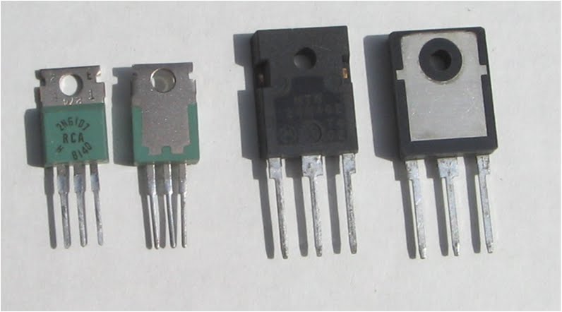
2N3055, pictured in Figure 1. Also pictured is his smaller brother, the 2N3054.


Figure 1: 2N3055 and 2N3054 power transistors

Following are some key maximum ratings on the 2N3055 power transistor:
  • VCEO = 60V
  • VCBO = 100V
  • VEBO= 7V
  • IC = 15A
  • PD = 115W
  • hfe= 45 typical
  • fT = 1.5 MHz
  • Thermal resistance = 1.5 oC/W
  • TJ= 200 oC
  • Package: TO-3 (now TO-204AA)
  • Polarity: NPN
  • Material/process: Silicon diffused junction hometaxial-base structure


Diffused junction silicon transistors made major inroads in the early 1960’s ultimately making the germanium power transistors obsolete.  One huge improvement using silicon, especially for power transistors, is the junction temperature, which is generally rated for 200 oC.  This allowed operating at much higher ambient temperatures and at higher power levels when compared to germanium. 

While the alloy junction process being used for the early germanium transistors favored making PNP transistors, the diffused junction process on silicon favored making NPN transistors somewhat more. Silicon diffused junction NPN transistors are much more prevalent than PNP devices, and the PNP complements to NPN devices, where available, are more costly.  

The diffusion process made a giant leap in transistor mass production possible. Many transistors could now be made at once on a larger silicon wafer, greatly reducing the cost. The more precise nature of the diffusion junction over the alloy junction also improved performance. As one example, tor the 2N3055 the transition frequency increased roughly another order of magnitude over the 2N1532 germanium alloy junction transistor in part 1, to 1.5 MHz.  

The hometaxial-base structure is a single simultaneous diffusion into both sides of a homogenously-doped base wafer, one side forming the collector and the other side the emitter. A pattern on the emitter side is etched away around the emitter, down to the P-type layer, to form the base. The emitter is left standing as a plateau or “mesa” above the base.

The 2N3054 was electrically identical to the 2N3055 except for its lower current and power capabilities. It’s smaller TO-66 package however was never very popular and was quietly phase out in the early 1980’s, sometimes along with some of the devices that were packaged in it!

Process improvements beyond the single diffused hometaxial-base structure continued through the 1960s with silicon transistors, including double diffused, double- and triple diffused planar and epitaxial structures. The epitaxial structure is a departure from the diffused structures in that features are grown onto the top of the base wafer. With greater control of doping levels and gradients, and more precise and complex geometries, the performance silicon power transistors continued to improve in most all aspects.

Plastic-packaged power transistors have for the most part come to displace hermetic metal packages like the TO-3 (TO-204AA), first due to the lower cost of the part and second, with simpler mounting, reducing the cost and labor of the products they are incorporated into. One drawback of most of the plastic-packaged power devices is their maximum temperature rating has been reduced to typically 150 oC, taking back quite a bit of temperature headroom provided by the same devices in hermetic metal packages. Sometimes there is a price to be paid for progress! Pictured in figure 2 are two (of many) popular power device packages, the smaller TO-220AB and the larger TO-247.

Figure 2: TO-220AB and TO-247 power device plastic packages

It’s pretty fascinating to see how transistors and the various processes used to manufacture them evolved over time. In these two posts I’ve hardly scratched the surface of the world of power transistors and power devices. For one there is a variety of other transistor types not touched upon, including a variety of power FETs. Power FETs have made major inroads in all kinds of applications in power supplies. Also work continues to provide higher power devices in surface mount packages. These are just a couple of numerous examples, possibly something to write about at a future date!


References: “RCA Transistor Thyristor & Diode Manual” Technical Series SC-14, RCA Electronic Components, Harrison, NJ 

Friday, August 31, 2012

To autoscale, or not to autoscale: that is the question!

While the primary focus of this blog is power, this post is about a topic that applies beyond just power: autoscale. I want our readers to comment on this topic:

 Should a test equipment user use the autoscale button or not? If so, why? If not, why not?

How is autoscale related to power, you ask? One of our Agilent power products, the N6705B DC Power Analyzer, has a build-in scope-like function with an autoscale button. The built-in scope is useful for measuring things like dynamic current flowing into a device or for looking at the response to an arbitrary waveform that can also be generated with the same product. To autoscale in Scope View mode, you push an N6705B front panel Autoscale button to automatically scale the vertical and horizontal axes to show you the waveforms on the scope screen.

While this may seem like a convenient feature, there are times when using autoscale on any instrument (like an oscilloscope) does not result in the display that you want. And some signals cannot be captured with an autoscale feature. The signal must be repetitive and typically meet certain minimum vales of voltage, frequency, and duty cycle. But more importantly, using autoscale eliminates having to think about the signals you are trying to observe. While this may seem like an advantage, I think it makes us lazy and less likely to understand what we are doing.

These days, we have grown too accustomed to just pushing a button to accomplish a task. We push a button to heat our food using a microwave. We push a button to cool our homes using our central air conditioning thermostat. We push a button to turn on our computers, get food, candy, and drinks from vending machines, get cash from an ATM, start our (modern) cars. We push buttons all day long! But when it comes to test and measurement equipment, we are trying to gain insight into the circuit or device we are analyzing. And I believe that insight starts with thinking about the waveforms we are trying to display. Thinking about what the waveshape is supposed to look like…how to trigger on the signal….what the approximate maximum voltage (or current or power) is….whether or not this is a repetitive waveform or a single event. Thinking about these things brings us closer to the insight we want to glean from the signals we examine. And ultimately, it is that insight that we seek. So just pushing a button to get a signal on a scope screen provides us with little insight; in fact, it could bias our thinking into mistakenly believing that what we are seeing is correct because we did not bother to think about what the waveforms are supposed to look like ahead of time!

So I say “no”, a test equipment user should not use the autoscale button for the reasons stated above. In fact, for years, I have trained new engineers and some of our sales people, and I have been known to say on more than one occasion, “No self-respecting engineer would ever hit the autoscale button!” Of course, I am only half-serious about this statement, but I think it supports my view that it is useful to think about what you expect on the scope before just viewing the waveforms. Of course, you should ALWAYS think about whether or not what you see on the display is expected and makes sense. After all, why else would you look at the signals?

What do YOU think???

Please comment below.

Power Supply Resolution versus Accuracy


One of the questions that we have received on the support team quite a few times and something that confused me when I started at Agilent is the concept of our resolution supplemental characteristic versus our accuracy specification.  I sat down with my colleague Russell and we wanted to do a simple explanation of the differences. 

If you look at our power supply offering, there is always an accuracy specification and a resolution supplemental characteristic for both programming and measurement.  For the purposes of this blog post, we are going to look at the programming accuracy (0.06% + 19 mV) and programming resolution (3.5 mV) of the N6752A High Performance DC Power Module.  Please note that these same explanations apply to the measurement side as well but for the sake of brevity we will be sticking to programming in our example.  

Let’s start by talking about resolution.  Our power supplies use Digital to Analog Converters (DACs) to take the user inputted settings and convert them to analog signals that set a programming voltage that will interact with the control loop of the power supply to set the output.  The resolution supplemental characteristic represents one single count of the DAC.  This is also known as the Least Significant Bit (LSB).  What this means for our end user is that the smallest step they can make between two settings on the unit is the programming resolution number.  In our example, the N6752A can be set to 0.9975 V, 1.001 V, 1.0045 V, etc.  These are all multiples of 3.5 mV and any setting that falls between two DAC counts will be put into the nearest count.  If the user tried to set the N6752A to 1 V, the power supply will actually be set to 1.001 V since that is the nearest count.  This is also known as quantization error. 

The accuracy specification always includes an error term for the quantization error.  This is typically half of the resolution supplemental characteristic.  The accuracy specification also includes many other factors such as DAC accuracy, DAC linearity, offset error of operational amplifiers, gain errors of the feedback loops, and temperature drift of components.   The accuracy will always be worse than the resolution since it includes all of the factors listed above as well as the term for the quantization error.  You can definitely see this in the N6752A where the resolution is 3.5 mV and just the offset of the accuracy specification not including the gain term is 19 mV which is more than 5 times greater than the resolution. 

I hope that this was helpful.   If there are any questions, please leave comments here or on our forum at Agilent Discussion Forums